


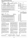

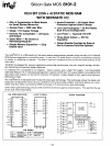

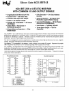

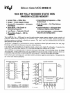

SILICON GATE MOS 8101-2
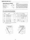
A.C. Characteristics
READ CYCLE TA =
o°c
to
70°C,
Vee
=
5V
±5~/~,
unless otherwise specified.
Symbol
Parameter
=I
Min.
Typ.
Max.
Unit
Test Conditions
--
~--_._---
tRey
Read Cycle
~
ns
-----
.-
--.--
tA
Access
Time
850
ns
____
._.
__
u.
___________
~---
~._----~._---
teo
Chip Enable
To
Output
6~._~~
(See below)
--_._-_
..
_----
too
Output
Disable
To
Output
r
550
ns
._-----.
-'-----
---_._-----
~-
200~--~~-1
tOF
[1]
Data
Output
to
High Z State 0
--
tOH
Previous Data Read Valid I
0
ns i
after
change
of
Address
WRITE CYCLE
Symbol
Parameter
I
Min.
Typ.
Max.
Unit
Test
Conditions
tweY
Write
Cycle
i
850
ns
tAW
Write
Delay
,
150
ns
tew
Chip
Enable
To
Write
-T
750
ns
(See
below)
tDW
Data Setup
1
500
ns
--
tOH
Data
Hold
100
ns
Write
Pulse
---_...
_----
--j--------
t-------
,...--'
twp
!
630
ns
tWR
Write
Recovery
:
50
I
ns
i
,
_---L-
A.
C.
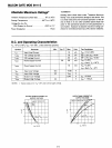
CONDITIONS OF TEST
Capacitance T
A
=
25°C,
f = 1
MHz
Input
Pulse Levels: +0.65
Volt
to
2.2
Volt
Input
Pulse Rise and Fall Times: 20nsec
1
TTL
Gate and C
L
~.:
100pF
Timing
Measurement Reference Level:
Output
Load:
1.5
Volt
-
Symbol
Test
Limits
(pF)
!
Typ.
Max.
C
IN
I
nput
Capacitance
4
8
~-
(All
Input
Pins) V
IN
=
OV
CoUT
Output
Capacitance
V
OUT
=
OV
8 12
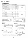
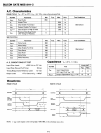
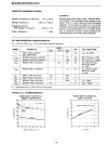
Waveforms
READ CYCLE
WRITE CYCLE
l2]
ADDRESS
==:>c
CE2 -
......
-....Il-
t
co
--.
I
CE2 /
-----"
DATA
IN
'\
'00
~.
/'OH
I
'--
-..J
t
A
•
t
OF
11;
.'
DATA
-
-1---
- - - -
-y
IJATAOUT
OUT
__
j
..A
V_A_L_ID
_
ODJ
•
tDf'
j.
- -
.--.,
t
OH
/.-·-
=x
~_~_~:_L_I~
-_
.
__
...
:,
t
tow
---
.-.
tAW
;.....--
tw
~
RW
'\
~p
-J
...
R !
. I
NOTES:
1.
tDF
is
with
respect
to
the
trailing
edge
of
CE1,
CE2,
or
OD,
whichever
occurs
first.
2.
During
the
write
cycle,
00
is
a
logical
1
for
common
1/0
and
"don't
care"
for
sepJ~ate
I/O
operation.
3.
00
should
be
tied
low
for
separate
I/O
operation.
00
(COMMON
lID)
131
5-69