


The
following pages will cover
the
detailed design
of
the CPU Module
with
the
8080.
The
three
Busses (Data,
Address
and
Control) will be developed
and
the
intercon-
nection
to
Memory
and
I/O will be shown.
Design philosophies
and
system architectures pre-
sented
in
this
manual are
consistent
with
product
develop-
l"M
ment
programs
underway
at
INTEL
for
the
MCS-80. Thus,
the
designer
who
uses this manual as a guide for his
total
system engineering
is
assured
that
all new developments
in
components
and software
for
MCS-80 from INTEL will be
compatible
with
his design
approach.
the
design
and
to
achieve
operational
characteristics
that
are as close as possible
to
those
of
the
8224
and
8228.
Many auxiliary timing
functions
and
features
of
the
8224
and
8228
are
too
complex
to
practically
implement
in
standard
components,
so
only
the
basic
functions
of
the
8224
and
8228
are generated. Since significant benefits
in
system timing
and
component
count
reduction
can be
realized by using
the
8224
and
8228,
this
is
the
preferred
method
of
implementation.
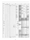
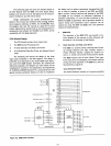
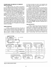
1. 8080
CPU
CPU
Module Design
The
CPU Module
contains
three
major areas:
1.
The
8080
Central Processing
Unit
2. A Clock
Generator
and
High Level Driver
3. A bi-directional Data Bus Driver
and
System Control
Logic
The
following will discuss
the
design
of
the
three
major areas
contained
in
the
CPU Module. This design
is
presented as
an
alternative
to
the
Intel®
8224
Clock Gener-
ator
and Intel
8228
System Controller. By studying
the
alternative
approach,
the
designer can
more
clearly see
the
considerations involved
in
the
specification and engineering
of
the
8224
and
8228.
Standard
TTL
components
and Intel
general
purpose
peripheral devices are used
to
implement
2.
The
operation
of
the
8080
CPU was covered
in
pre-
vious
chapters
of
this manual,
so
little reference will
be made
to
it
in
the
design
of
the
Module.
Clock Generator and High Level Driver
The
8080
is
a
dynamic
device, meaning
that
its inter-
nal storage
elements
and
logic
circuitry
require a
timing reference (Clock), supplied
by
external cir-
cuitry,
to
refresh
and
provide timing
control
signals.
The
8080
requires
two
(2) such Clocks.
Their
wave-
forms
must
be non-overlapping,
and
comply
with
the
timing
and
levels specified
in
the
8080
A.C.
and
D.C.
Characteristics, page 5-15.
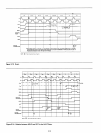
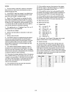
Clock Generator Design
The
Clock
Generator
consists
of
a crystal
controlled,
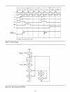
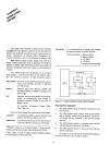
2
25
GND
AO
AO
+5V
20
26
Al
Al
11
27
-5V
A2
A2
+12V
28
A3
29
30
A3
A4
A4
AS
31
AS
A6
32
A6
8080
33
CPU
A7
A7
A8
34
A8
ADDRESS BUS
13
35
SYSTEM
DMA
REO.
HOLD
A9
A9
Al0
1
Al0
All
40
All
14
A12
37
A12
SYSTEM
INT.
REO.
tNT
A13
38
~13
INT.
ENABLE
16
INTE
A14
39
A14
A15
36
A15
WR
18
XTAL
17
0
DBIN
HLDA
21
22
10
ct>1
DO
15
9
eJ>2
01
02
8
CLOCK
24
WAIT
03
7
BI-DIREC-
WAIT
REO.
GENERATOR
23
3
TIONAL
DATA
BUS
DRIVER
READY
04
BUS
DRIVER
4
12
05
SYS. RESET
RESET
5
06
19
07
6
SYNC
1
STATUS STROBE
SYSTEM
CONTROL
Figure 3-2. 8080
CPU
Interface
3-2