


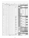
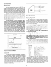

Auxiliary Timing Signals
and
Functions
The
Clock
Generator
can also be used
to
provide
other
signals
that
the
designer can use
to
simplify
large system timing
or
the
interface
to
dynamic
memories.
Functions such as power-on reset, synchronization
of
external requests (HOLD, READY, etc.) and single
step, could easily be
added
to
the
Clock Generator
to
further
enhance
its capabilities.
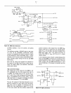
For instance,
the
20
MHZ signal from
the
oscillator
can be buffered so
that
it could provide
the
basis for
communication baud rate generation.
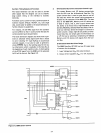
The Clock Generator diagram also shows
how
to
gen-
erate an advanced timing signal
(l/>1A)
that
is
handy
to
use
in
clocking
"0"
type
flipflops
to
synchronize
external requests. It can also be used
to
generate a
strobe (STSTB)
that
is
the
latching signal for
the
sta-
tus information which
is
available on
the
Data Bus
at
the
beginning
of
each machine cycle. A simple gating
of
the
SYNC signal from
the
8080
and
the
advanced
(l/>1A)
will
do
the
job. See Figure 3-3.
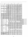
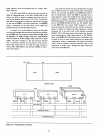
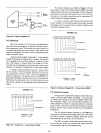
3.
Bi-Directional Bus Driver
and
System
Control
Logic
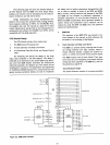
The
system Memory
and
I/O devices
communicate
with
the
CPU over
the
bi-directional Data Bus.
The
system Control Bus
is
used
to
gate
data
on
and
off
the
Data Bus within
the
proper
timing sequences as
dictated by
the
operation
of
the
8080
CPU. The data
lines
of
the
8080
CPU, Memory and I/O devices are
3-state
in
nature,
that
is,
their
output
drivers have
the
ability
to
be forced
into
a high-impedance mode
and are, effectively, removed
from
the
circuit. This
'3-
state bus
technique
allows
the
designer
to
construct
a
system
around
a single, eight (8)
bit
parallel, bi-direc-
tional Data Bus and simply gate
the
information on
or
off
this bus by selecting
or
deselecting (3-stating)
Memory
and
I/O devices
with
signals
from
the
Con-
trol Bus.
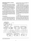
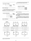
Bi-Directional Data Bus Driver Design
The
8080
Data Bus
(07-00)
has
two
(2) major areas
of
concern for
the
designer:
1.
Input
Voltage level
(V
1H
)
3.3
volts minimum.
2.
Output
Drive Capability (tOL) 1.7 rnA maximum.
OBO
OB1
OB2
OB3
OB4
DB5
DB6
DB7
BUSEN
-
DO
2,4
r-
3
01
5,7
r-
6
9,11r-
8216
10
02
03
12,
14
r-
13
OlEN
CS
15?
«1
04
2,4]
3
05
5,7
r-
6
9,11r-
8216
10
06
07
12,
14
r-
13
OlEN
CS
OBIN
~I
15)'
?1
...,
3
4
INTA
Q.»--
I....--
5 6
WO
-
-
0
7
8 STACK
-
9
8212
10
HLTA
-
16
15 OUT
~
Q.»--
18
17
M1
-
20
191NP
22
21
MEMR
c=[y--
------!1
12
[13
STSTB
Vee
-
WR
......
1
I
......
-
-
--(>0.-=0--
808
Figure 3-5.
8080
System Control
3-4