SILICON GATE MOS
81078·4
ADDRESS
CAN
CHANGE
0
14-----------t
ce
(300)
----------~
\'JH
--
...
--~-+------------------------_t-;-.....,r_----.,...--
tAC(O)-
.......
-~
V
,HC
----+-----+-I..-oI!""!!-----------------------
.....
CE
t
cO
(2S0)
---------.1
.
._----..--
t:(~
~
OoUT
.....
IMP~6~NCE
1-_....iI
...
V_A_L_ID_-_-_-:.::=~~
~:~~~:~
VoL
- -
-II.~-----------------
t
ACc
(270)
.1
tCF(O) :
ADDRESS
AND~
\'IL
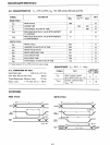
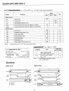
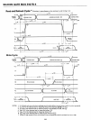
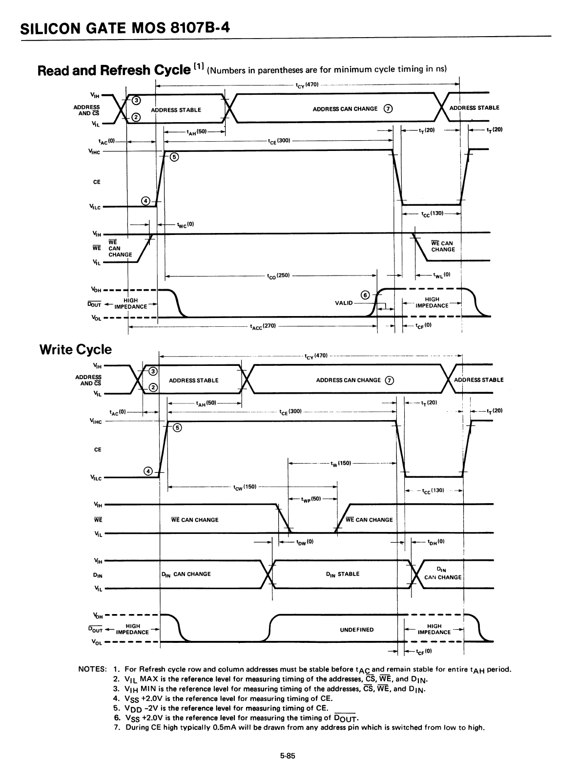
Read and Refresh Cycle [1) (Numbers in parentheses are
for
minimum
cycle
timing
in
ns)
~--------------
t
Cy
(470)
----------------------~
------.
-----..1
..-----t
w
'1S0)----
ADDRESS
CAN
CHANGE
CD
- t
ce
(300)
_._---
._----_._--~
------
t
Cy
(470)
---
------
ADDR
ESS
STABLE
..----
t
AH
(SO)-----.
14--------
t
cw
(1S0)
-----4-----~
DtN
CAN
CHANGE
®
®
DIN
V
1H
------~-----------~
CE
o
V'LC
----
.....
-..11
WE
CAN
CHANGE
V
1HC
--------i-
~~~----------------------
.....
®
\'JH
------+----------~
V
1L
------t--------------I--
...
----
....
-----~~------_t_---
\'JL
------t-----------~
\'JH
ADDRESS
ANDCS
\'JL
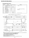
Write Cycle
'bH-------
-----~
D
OUT
'-IMP~~~~CE
-.~_
.......
--I11111111'.---
U_N_D_E_FI_N_E_D
__
......
_IM_P~_ri~~_CE
__
'
VOL
---
- -
--,.-
teF(O)
NOTES: 1.
For
Refresh cycle
row
and
column
addresses must be stable before
tAC
and remain stable
for
entire
tAH
period.
2.
VIL
MAX
is
the
reference level
for
measuring
timing
of
the
addresses,
CS,
WE, and
DIN.
3.
VIH
MIN
is
the
reference level
for
measuring
timing
of
the
addresses, CS, WE, and
DIN.
4.
VSS
+2.0V
is
the
reference level
for
measuring
timing
of
CEo
5.
VOO
-2V
is
the
reference level
for
measuring
timing
of
CEo
6. VSS
+2.0V
is
the
reference level
for
measuring
the
timing
of
00UT.
7.
During
CE
high
typically
O.5mA
will
be
drawn
from
any address
pin
which
is
switched
from
low
to
high.
5-85


