101
CHAPTER 4 I/O PORTS
■
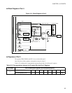
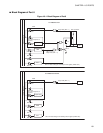
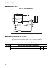
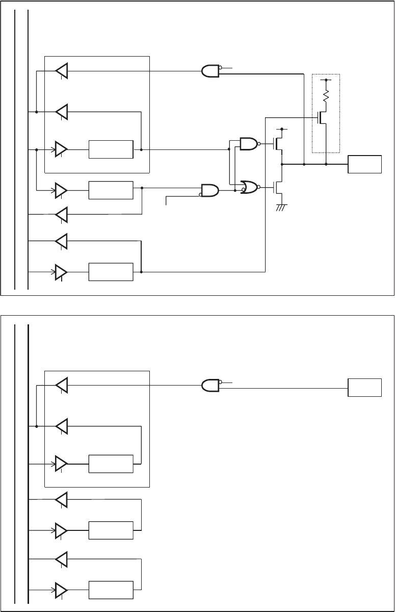
Block Diagram of Port 6
Figure 4.6-1 Block Diagram of Port6
DDR
P-ch
N-ch
PDR
PUL
Internal data bus
PDR read
PDR read
(when read-modify-write is
performed)
Output latch
PDR write
DDR write
PUL read
Stop mode (SPL = 1)
Pull-up resistor
Pin
Stop mode (SPL = 1)
PUL write
For MB89202/V201
PDR
DDR
Internal data bus
PDR read
PDR read
(when read-modify-write is
performed)
Output latch
PDR write
DDR read
Pin
Stop mode (SPL = 1)
DDR read
For MB89F202/F202RA
PUL
PUL read
PUL write
DDR read
SPL: Pin state setting bit of standby control register (STBC: SPL)
SPL: Pin state setting bit of standby control register (STBC: SPL)


