


81
CHAPTER 4 I/O PORTS
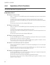
Table 4.2-3 lists the functions of the port 0 registers.
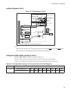
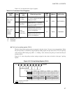
● Port 0 pull-up setting register (PUL0)
The bits of the pull-up setting register correspond to the pins of port 0 in one-to-one correspondence. When
the pull-up resistor is selected by using the pull-up setting register, the pin will be at "H" level (pull-up
state) instead of Hi-Z during stop (SPL = 1). During a reset, however, the pull-up is invalid and the pin
remains at Hi-Z.
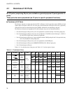
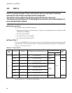
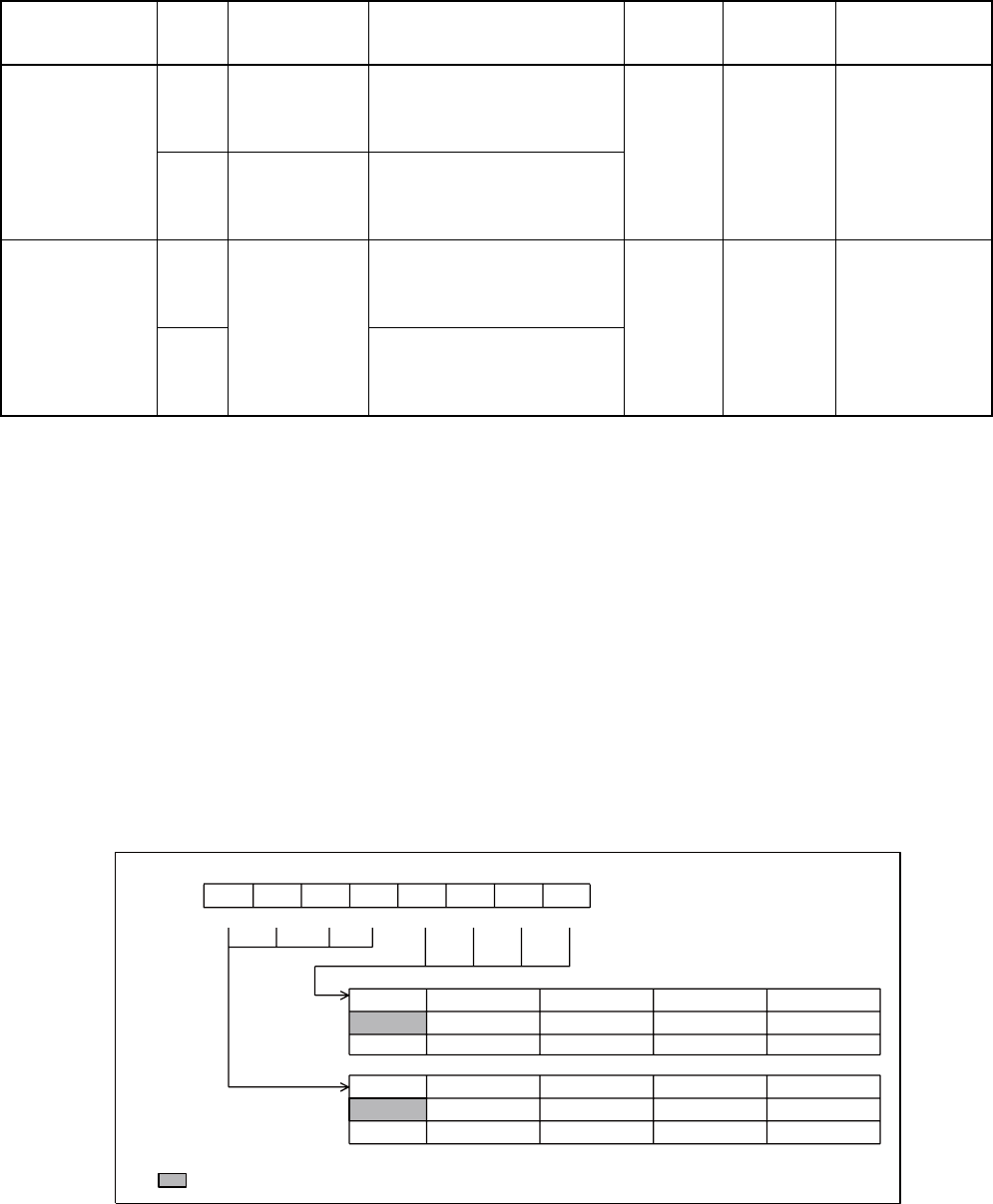
Figure 4.2-2 shows the pull-up resistor settings assigned to the values of the bits of the port 0 pull-up
register.
Figure 4.2-2 Pull-up Resistor Settings (PUL0)
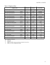
Table 4.2-3 Functions of Port 0 Registers
Register
name
Data
When being
read
When being written
Read/
Write
Address Initial value
Port 0 data
register (PDR0)
0
Pin state is
"L" level.
Output latch of "0" is set and
"L" level is output to the pin
in output port mode.
R/W 0000
H
XXXXXXXX
B
1
Pin state is
"H" level.
Output latch of "1" is set and
"H" level is output to the pin
in output port mode.
Port 0 data
direction
register (DDR0)
0
Read
prohibited
(write only)
Output transistor operation
is disabled and the pin is set
to serve as an input pin.
W 0001
H
00000000
B
1
Output transistor operation
is enabled and the pin is set
to serve as output pin.
R/W: Readable/Writable
W : Write only
X : Undefined
PUL03
PUL02 PUL01
PUL00
0
1
PUL07 PUL06 PUL05
PUL04
0
1
bit7 bit6 bit5 bit4 bit3 bit2 bit1 bit0
0070
H
PUL07
PUL06
PUL05
PUL04 PUL03 PUL02 PUL01 PUL00
00000000
B
R/W R/W R/W R/W R/W R/W R/W R/W
R/W
Address
Initial value
P03 pull-up OFF
P02 pull-up OFF P01 pull-up OFF P00 pull-up OFF
P03 pull-up ON P02 pull-up ON
P01 pull-up ON P00 pull-up ON
P07 pull-up OFF P06 pull-up OFF P05 pull-up OFF P04 pull-up OFF
P07 pull-up ON P06 pull-up ON
P05 pull-up ON P04 pull-up ON
: Readable/Writable
: Initial value