


xi
Main changes in this edition
Page Changes (For details, refer to main body.)
-
-
The followings product name is changed.
(MB89202 → MB89202/F202RA)
The followings term is changed.
(source oscillation → oscillation frequency)
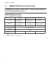
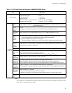
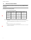
6 1.3 Differences between
Models
"Notes:" is changed.
(The followings sentence is deleted.
"
• At turning on the power, when the device is used without inputting the external
reset, select "reset output supported" and "power-on reset supported" by mask
option.")
The followings package is changed in Table 1.3-1.
(FPT-34P-M03 → FPT-32P-M03)
12 1.7 Pin Functions RST
pin in Table 1.7-1 is changed.
19 2.1 Precautions on
Handling Devices
"● External pull-up for the External Reset Pin (RST
) of MB89F202/F202RA" is
changed.
24 3.1.1 Specific-purpose
Areas
The summary is changed.
"■ General-purpose Register Area (address: 0100
H
to 01FF
H
)" is changed.
"■ Vector Table Area (Address: FFC0
H
to FFFF
H
)" is changed.
44 3.5 Reset "● Power-on reset" is changed.
"Note:" is deleted.
56 3.6.3 System Clock
Control Register (SYCC)
Figure 3.6-5 is changed.
57 Table 3.6-1 is changed.
130 6.3 Watchdog Control
Register (WDTC)
Figure 6.3-1 is changed.
186 8.6 Explanation of
Operations of Interval
Timer Functions
"● 8-bit mode"is changed.
(The followings sentence is deleted.
"The initial value of the square wave output is "L" level. The square wave output is
initialized by writing "0" to the TSTR bit of the timer control register (TCR).")
264 12.3 Pins of A/D
Converter
"■ Block Diagram of the Pins Related to the A/D Converter" is changed.
("Note:" is deleted.)
308 13.6.2 Reception
Operations (Operating
Mode 0, 1, or 3)
"■ Reception Operations (Operating Mode 0, 1, or 3)" is changed.
("Note:" is changed.)