


407
INDEX
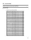
Command Sequence
Command Sequence Table................................ 361
COMR
PWM Compare Register (COMR)..................... 145
Condition Code Register
Configuration of the Condition Code Register (CCR)
............................................................ 29
Configuration
Configuration of Memory Space.......................... 22
Configuration of the Condition Code Register (CCR)
............................................................ 29
Configuration of the General-purpose Registers
............................................................ 32
Configuration of the Interrupt Level Setting Registers
(ILR1 to ILR4) ..................................... 36
Configuration of the Register Bank Pointer (RP)
............................................................ 31
Configuration of the Reset Flag Register (RSFR)
............................................................ 45
Configuration of the System Clock Control Register
(SYCC)................................................ 56
Dedicated Register Configuration........................ 27
Controlling Acceptance
Bits for Controlling Acceptance of Interrupts
............................................................ 30
Counter
Counter Function ............................................. 165
Counter Function Operation.............................. 189
Program Example of Counter Function .............. 202
CPU Reads
States of Pins after the CPU Reads the Mode Data
............................................................ 50
D
Data Setting Register
Data Setting Register (WRDR).......................... 351
DDR
Registers of Port 4.............................................. 91
Registers of Port 5.............................................. 95
Registers PDR0, DDR0, and PUL0 of Port 0 ........ 79
Registers PDR3, DDR3, and PUL3 of Port 3 ........ 85
Registers PDR6, DDR6, and PUL6 of Port 6 ...... 102
Registers PDR7, DDR7, and PUL7 of Port 7 ...... 108
Detailed Explanation
Detailed Explanation of Flash Memory Write/Erase
.......................................................... 367
Diagram
Diagram for State Transition in Standby Mode
............................................................ 68
DIP-32P-M06
Package Dimension of DIP-32P-M06 .................. 10
Pin Assignment of DIP-32P-M06 .......................... 8
E
EIC
External Interrupt Control Register 1 (EIC1)
..........................................................232
External Interrupt Control Register 2 (EIC2)
..........................................................235
EIE
External Interrupt Circuit 2 Control Register (EIE2)
..........................................................250
EIF
External Interrupt 2 Flag Register (EIF2) ............252
Erase
Automatic Write/Erase......................364, 365, 366
Detailed Explanation of Flash Memory Write/Erase
..........................................................367
Erasing
Automatic Erasing............................................363
Erasing All Data (Erasing Chips) .......................371
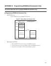
Writing to/Erasing Flash Memory ......................358
Erasing All Data
Erasing All Data (Erasing Chips) .......................371
Erasing Chips
Erasing All Data (Erasing Chips) .......................371
Evaluation Chip
Programming EPROM with Evaluation Chip
..........................................................401
Example
Example of Operations of 12-bit PPG Timer Functions
..........................................................219
Exercise Caution
Exercise Caution when Changing Edge Polarity
Selection.............................................238
Explanation
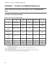
Explanation on Addressing................................383
Explanation on the Codes Representing Instructions
..........................................................381
Explanation on the Items of Instructions’List
..........................................................382
External Interrupt
Association between the Interrupt Enable Bits for
External Interrupt Circuit 2 and the External
Interrupt Pins.......................................248
Block Diagram of Circuitry Terminating at the Pins
Associated with External Interrupt Circuit 1
..........................................................230
Block Diagram of Circuitry Terminating at the Pins
Associated with External Interrupt Circuit 2
..........................................................247
Block Diagram of External Interrupt Circuit 1
..........................................................227
Block Diagram of External Interrupt Circuit 2
..........................................................245
Functions of External Interrupt Circuit 1.............226