370
CHAPTER 17 FLASH MEMORY
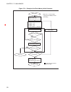
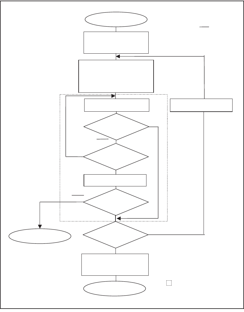
Figure 17.5-1 Example of the Flash Memory Write Procedure
Data
Data
Data
0
1
Data
Start writing*
Make sure +10V DC voltage
is applied at the RST pin before
start writing
*
FMCS: WE (bit5)
Enable flash memory write
Write command sequence
(1) FAAA <-- AA
(2) F554 <-- 55
(3) FAAA <-- A0
(4) Write address <-- Write data
Read internal address
Next address
Data polling (DQ7)
Timing limit (DQ5)
Read internal address
Data polling (DQ7)
Write error
Final address
NO
YES
FMCS: WE (bit5)
Write-disable flash memory.
Complete writing
Confirm with the hardware
sequence flags.


