


321
CHAPTER 14 8-BIT SERIAL I/O
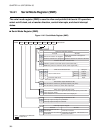
Table 14.4-1 Explanation of Functions of Each Bit in Serial Mode Register (SMR) (1/2)
Bit name Function
bit7
SIOF:
Interrupt request flag bit
• When 8-bit serial data is input or output during serial I/O operation, this
bit is set to "1". When this bit and the interrupt request allowance bit
(SIOE) are "1", an interrupt request is output.
• Setting this bit to "0" clears it, while setting it to "1" does not affect this
bit or implement any changes.
bit6
SIOE:
Interrupt request
allowance bit
This bit is used to allow and prohibit interrupt request output to the CPU.
When this bit and the interrupt request allowance bit (SIOF) are "1", an
interrupt request is output.
bit5
SCKE:
Shift clock output
allowance bit
• This bit is used to control shift clock I/O.
• When this bit is "0", the P30/UCK/SCK pin functions as the shift clock
input pin. When "1", it functions as the shift clock output pin.
Notes:
• To use the P30/UCK/SCK pin as the shift clock input pin, it must be set
as an input port. Also select the external shift clock with the shift clock
selection bits (Set the CKS1 and CKS0 bits to 11
B
).
• For shift clock output (SCKE bit = 1), select an internal shift clock (do
not set the CKS1 and CKS0 bits to 11
B
).
Notes:
• When shift clock output is allowed (when this bit is "1"), the P30/UCK/
SCK pin functions as the UCK/SCK output pin irrespective of the
general-purpose port (P30) state.
• When using the P30/UCK/SCK pin as a general-purpose port (P30), set
its pin as the shift clock input pin (set this bit to "0").
bit4
SOE:
Serial data output
allowance bit
When this bit is "0" the P31/UO/SO pin functions as a general-purpose port
(P31). When "1", the P31/UO/SO pin functions as the serial data output pin
(UO/SO).
Note:
When serial data output is allowed (when this bit is set to "1"), the P31/
UO/SO pin functions as the UO/SO pin irrespective of the general-
purpose port (P31) state.
bit3,
bit2
CKS1, CKS0:
Shift clock selection bits
• These bits are used to select three internal shift clocks or one external
shift clock.
• When these bits are not 11
B
, an internal shift clock is selected. When the
shift clock output allowance bit (SCKE) is "1", a shift clock is output
from the UCK/SCK pin.
• When these bits are 11
B
, the external clock is selected. When the P30/
UCK/SCK pin is set as the shift clock input pin, a shift clock is input
from the UCK/SCK pin (when the SCKE bit and bit0 of the DDR3 are
"0").