


410
INDEX
Program Example for External Interrupt Circuit 2
..........................................................256
Reception Interrupt...........................................303
Register and Vector Table Related to 8/16-bit Capture
Timer/Counter of Interrupts..................184
Register and Vector Table Related to Interrupts from
Time-base Timer.................................121
Register and Vector Table Related to the Interrupt of
the A/D Converter ...............................272
Register and Vector Table Related to the Interrupts of
an 8-bit PWM Timer............................147
Register Associated with Interrupt Generation by
External Interrupt Circuit 1 and Vector
Table..................................................238
Register Associated with Interrupt Generation by
External Interrupt Circuit 2 and Vector
Table..................................................253
Registers Associated with External Interrupt Circuit 1
..........................................................231
Registers Associated with External Interrupt Circuit 2
..........................................................249
Stack Area for Interrupt Processing......................42
Stack Operation at the Beginning of Interrupt
Processing ............................................41
Stack Operation at the End of Interrupt Processing
............................................................41
Steps in the Interrupt Operation ...........................37
Transition to Standby Mode and Interrupt.............70
Transmission Interrupt......................................303
UART Interrupt Related Registers and Vector Table
Addresses...........................................303
Interrupt Enable Bits
Association between the Interrupt Enable Bits for
External Interrupt Circuit 2 and the External
Interrupt Pins ......................................248
Interrupt Level Setting Registers
Configuration of the Interrupt Level Setting Registers
(ILR1 to ILR4)......................................36
Interrupt Requests
Interrupt Requests from Peripheral Functions........34
Interval Timer
Interrupts when the Interval Timer Function is
Enabled..............................................121
Interrupts while Interval Timer Functions are Enabled
..........................................................147
Interval Timer Function ............................116, 162
Interval Timer Function Operation.....................185
Interval Timer Functions (Functions to Output
the Square Wave) ................................136
Operations of Interval Timer Function
(Time-base Timer)...............................122
Operations of the Interval Timer Functions.........148
Program Example of Interval Timer Function
..........................................................200
Program Example of Interval Timer Functions
..........................................................157
L
Level Detection
Functions of External Interrupt Circuit 2
(Level Detection)................................ 244
Lower Address Set Register
Lower Address Set Register (WRARL).............. 353
M
Mask
Mask Options .................................................. 400
MB89202/F202RA
Block Diagram of MB89202/F202RA Series.......... 7
Features of MB89202/F202RA Series.................... 2
MB89202/F202RA Series Models ......................... 4
Memory Access
Operations for Selecting Memory Access Mode
........................................................... 72
Memory Map
Memory Map..................................................... 23
Memory Space
Configuration of Memory Space.......................... 22
Mode
Cancellation of Standby Mode by an Interrupt
........................................................... 70
Diagram for State Transition in Standby Mode
........................................................... 68
Mode Data ........................................................ 72
Mode Fetch ....................................................... 49
Notes on Setting Standby Mode .......................... 70
Operation in Standby Mode and at Halfway Stop
......................................................... 197
Operations for Selecting Memory Access Mode
........................................................... 72
Operations in Active Mode ................................. 59
Operations in Each Clock Mode.......................... 58
Operations in Standby Mode............................... 63
Operations in the Standby Mode and at a Suspension
......................................................... 152
Operations Related to Sleep Mode....................... 64
Operations Related to Stop Mode ........................ 65
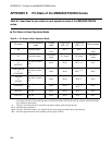
Pin States in Each Operation Mode.................... 402
Reception Operations (Operating Mode 0,1,or 3)
......................................................... 307
Reception Operations (Operating Mode 2 Only)
......................................................... 309
Single-chip Mode............................................... 72
States of Pins after the CPU Reads the Mode Data
........................................................... 50
Theory of Operation for Operating Mode 0,1,2, and 3
......................................................... 305
Transition to Standby Mode and Interrupt ............ 70
Transmission Operations in Operating Mode is
0,1,2,or 3............................................ 306