


264
CHAPTER 12 A/D CONVERTER
■
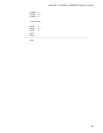
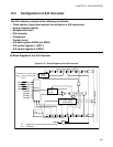
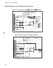
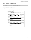
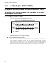
Block Diagram of the Pins Related to the A/D Converter
Figure 12.3-1 Block Diagram of P03/INT23/AN7 to P00/INT20/AN4 Pins
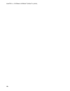
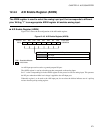
Figure 12.3-2 Block Diagram of P43/AN3 to P40/AN0 Pins
DDR
Pch
Nch
PDR
PUL
SPL: Pin status setting bit of the standby control register (STBC)
A/D converter
channel select
A/D converter enable bit
(only P00 to P03)
To the A/D
converter
analog input
To an external interrupt
From disabling an
external interrupt
PDR read
PDR read
Stop mode (SPL = 1)
(At read-modify-write)
Pull-up
resistor
Internal data bus
Output
latch
PDR write
DDR write
Pins
PUL read
PUL write
Stop mode (SPL = 1)
P00/INT20/AN4
P01/INT21/AN5
P02/INT22/AN6
P03/INT23/AN7
DDR
Pch
Nch
PDR
OUT
P40/AN0
P41/AN1
P42/AN2
P43/AN3
A/D converter
channel select
A/D converter
enable bit
To the A/D
converter
analog input
Stop mode (SPL = 1)
PDR read
Internal data bus
PDR read
(At read-modify-write)
Output
latch
PDR write
Pins
DDR write
OUT read
OUT write
Stop mode
(SPL = 1)
DDR read