


268
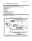
CHAPTER 12 A/D CONVERTER
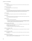
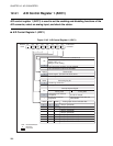
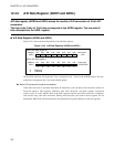
12.4.2 A/D Control Register 2 (ADC2)
A/D control register 2 (ADC2) is used to select an input clock, enable and disable an
interrupt and continuous activation.
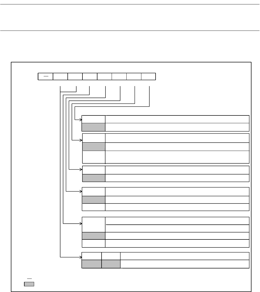
■ A/D Control Register 2 (ADC2)
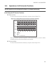
Figure 12.4-3 A/D Control Register 2 (ADC2)
1
RESV1
EXT
0
1
RESV2
0
ADIE
0
1
ADCK
0
1
RESV3 RESV4
00
bit7 bit6 bit5 bit4 bit3 bit2 bit1 bit0
0031
H
RESV4
RESV3 ADCK
ADIE
RESV2
EXT
RESV1
-0000001
B
R/W R/W R/W R/W R/W R/W R/W
R/W : Readable/ Writable
: Unused
: Initial value
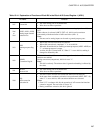
Address
Initial value
Reserved bit
Be sure to write "1" to this bit.
Bit for enabling continuous activation
Enables activation by setting the AD bit in the ADC1 register.
Enables continuous activation through the clock selected in the
ADCK bit.
Reserved bit
Be sure to write "0" to this bit.
Enabling an interrupt request bit
Disables the interrupt request output.
Enables the interrupt request output.
Selecting an input clock bit
Enabled only at continuous activation (EXT = 1)
From the time-base timer output (2
8
/F
CH
).
From the 8/16-bit capture timer/counter output (TO).
Reserved bits
Be sure to write 00
B
to these bits.