


333
CHAPTER 14 8-BIT SERIAL I/O
14.9 Notes on Using 8-Bit Serial I/O
This section provides notes on using the 8-bit serial I/O.
■ Notes on Using 8-bit Serial I/O
● Error at serial transfer start
The time at which serial I/O transfer is started with a serial transfer program (SMR: SST = 1) is
asynchronous with the time when the falling edge (output) or rising (input) edge of a shift clock occurs. For
this reason, the time that lasts until the first serial data is input or output is delayed by a maximum of one
cycle of the set shift clock.
● Malfunction due to noise
If external noise causes an extra pulse (pulse exceeding the hysteresis width) to be placed on a shift clock
during serial data transfer, the 8-bit serial I/O may malfunction.
● Notes on setting via program
• Write data to the serial mode register (SMR) and serial data register (SDR) only when the 8-bit serial I/
O is stopped (SMR: SST = 0).
• When starting or allowing serial I/O transfer (SMR: SST=1), do not change other bits of the SMR.
• If MSB first is set when a shift clock is used in external shift clock input, the highest bit level is output
as the SO pin output level. If LSB first is set, the lowest bit level is output as the SO pin output level.
MSB first and LSB first are set when the external shift clock is input. In this case, however, serial data
output must be allowed (SMR: SOE = 1) even if serial I/O transfer is stopped (SMR: SST = 0).
• If serial I/O transfer stop (SMR: SST = 0) and serial data transfer termination take place at the same
time during serial I/O operation, the interrupt request flag bit (SMR: SIOF) is not set to "1".
• If the SIOF bit is set to "1" and the interrupt request output allowance bit is enabled (SMR: SIOE = 1),
control cannot return from interrupt processing. Be sure to clear the SIOF bit.
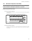
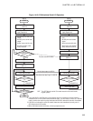
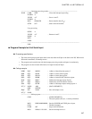
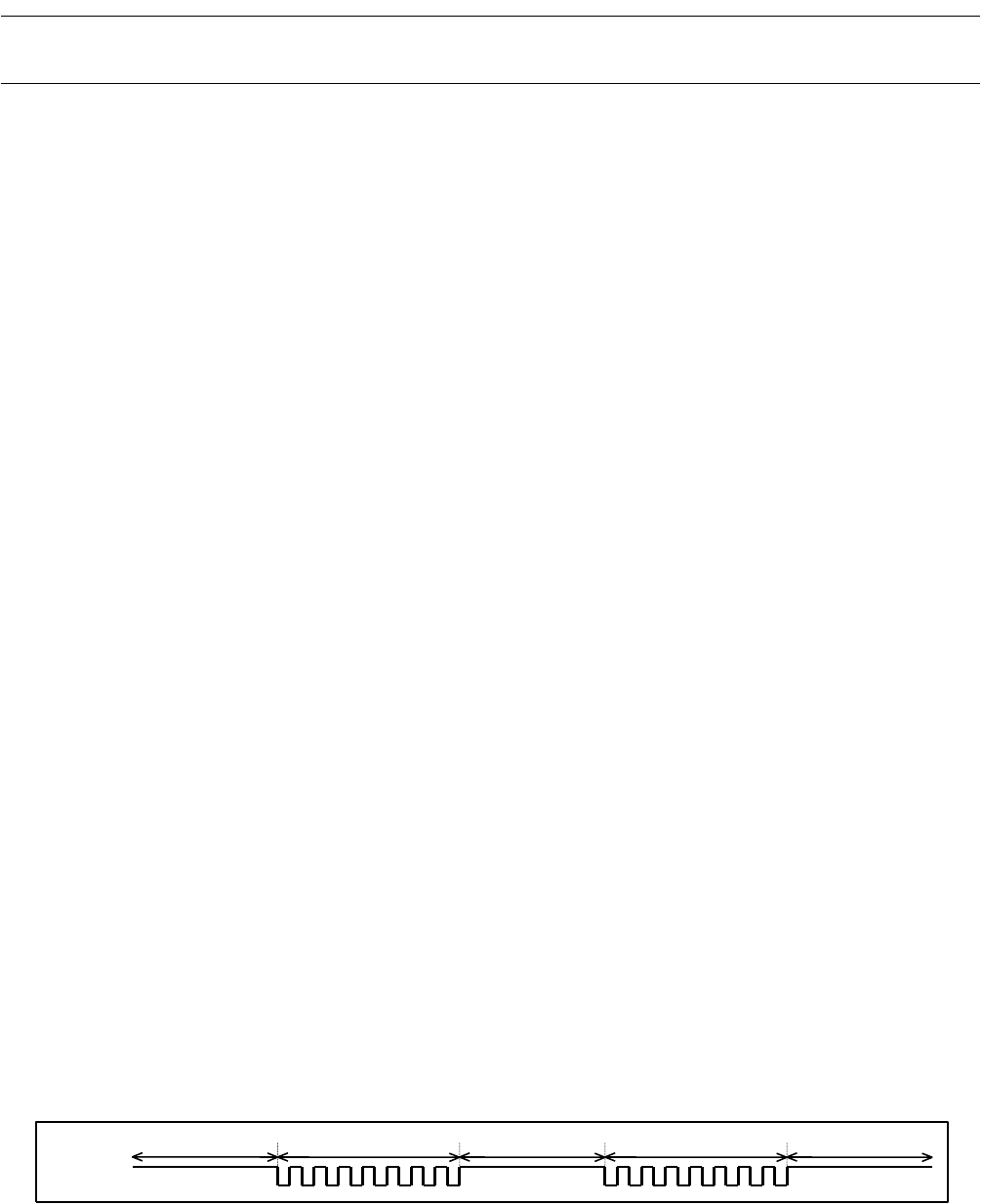
● Shift clock idle state
The external shift clock must maintain the "H" level during the wait time between one 8-bit data transfer
and another (idle state). When the internal shift clock is selected (SMR: CKS1, CKS0 = not 11
B
) and the
P30/UCK/SCK pin is used as the shift clock output pin (SMR: SCKE = 1), data is output at the "H" level in
the idle state.
Figure 14.9-1 shows the shift clock idle state.
Figure 14.9-1 Shift Clock Idle State
External
shift
clock
Idle state
8-bit data transfer
8-bit data transferIdle state Idle state