


263
CHAPTER 12 A/D CONVERTER
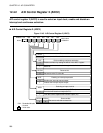
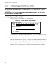
12.3 Pins of A/D Converter
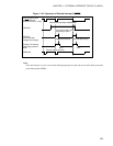
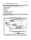
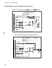
This section describes the pins related to the A/D converter and shows a block diagram
of the pins related to the A/D converter.
■ Pins Related to the A/D Converter
The pins related to the A/D converter are P03/INT23/AN7 to P00/INT20/AN4, and P43/AN3 to P40/AN0
pins.
● P03/INT23
/AN7 to P00/INT20/AN4 and P43/AN3 to P40/AN0
P03/INT23
/AN7 to P00/INT20/AN4, and P43/AN3 to P40/AN0 pins can be used as general-purpose I/O
ports (P03 to P00, and P43 to P40) and as analog inputs (AN7 to AN0).
[AN7 to AN0]
When A/D conversion functions are used, input the analog voltage to be converted to these pins. To
enable a pin as the analog input, set "1" to the bit that corresponds to the A/D enable register (ADEN),
set "0" to the bit that corresponds to the port data direction register (DDR0), and switch the output
transistor to OFF, and select one using the bit for selecting an analog input channel (ADC1: ANS0 to
ANS2). Even when the A/D converter is used, pins not used as analog inputs can be used as general-
purpose I/O ports.