


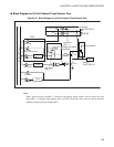
177
CHAPTER 8 8/16-BIT CAPTURE TIMER/COUNTER
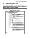
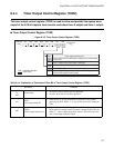
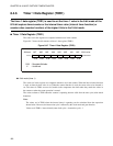
8.4.4 Timer Output Control Register (TCR2)
The timer output control register (TCR2) is used to allow and prohibit the square wave
output of the 8/16-bit capture timer/counter and select timer 0 output and timer 1 output.
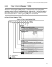
■ Timer Output Control Register (TCR2)
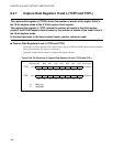
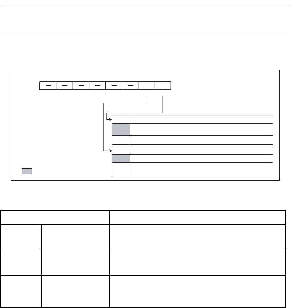
Figure 8.4-5 Timer Output Control Register (TCR2)
TSEL
0
PEN
0
bit7 bit6 bit5 bit4 bit3 bit2 bit1 bit0
PEN
TSEL
R/W R/W
R/W : Readable/Writable
: Initial value
1
1
Address
Initial value
Timer output selection bit
Timer 0 output in the 8-bit mode or output in the 16-bit mode
is selected.
Timer 1 output in the 8-bit mode is selected.
Port output enable bit
The P34/TO/INT10 pin acts as the general-purpose port (P34).
The P34/TO/INT10 pin acts as the square wave output pin
of the 8/16-bit capture timer/counter.
0020
H
------00
B
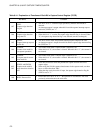
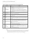
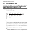
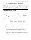
Table 8.4-4 Explanation of Functions of Each Bit in Timer Output Control Register (TCR2)
Bit name Function
bit7
to
bit2
Unused bits
• At read, the values of these bits are undefined.
• At write, these bits do not affect operation.
bit1
PEN:
Port output enable bit
• When this bit is "0", the P34/TO/INT10 pin acts as the general-
purpose port (P34). When "1", it acts as the square wave output pin
(TO).
bit0
TSEL:
Timer output selection bit
• When this bit is "0", timer 0 output in the 8-bit mode or output in the
16-bit mode is selected. In this case, data is output from the TO pin.
When "1", timer 1 output in the 8-bit mode is selected. In this case,
data is also output from the TO pin.