


281
CHAPTER 13 UART
■
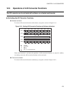
Serial Switch
UART and 8-bit serial I/O use the same pins, thus they cannot be simultaneously used. The serial switch
circuit needs be used to select either of them.
When UART is selected using the serial switch, P30/UCK/SCK is used as the UART serial clock I/O pin
(UCK), P31/UO/SO is used as the UART data output pin (UO), and P32/UI/SI is used as the UART data
input pin (UI).
Note:
In this chapter, the pin function switch and register functions are explained on the presupposition that
UART is selected using the serial switch circuit.
■
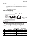
Choice of the Transfer Clock Rate
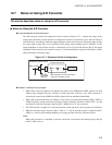
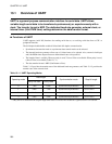
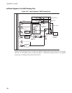
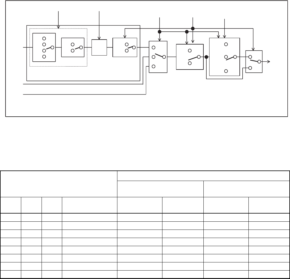
Figure 13.1-1 Baud Rate Generator and Serial Clock Generator
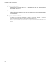
● Example of the baud rates selectable when the dedicated baud rate generator is used
Table 13.1-2 lists the baud rates selectable when the dedicated baud rate generator is used.
(1/2)
n
1
1/2
1/8
1/16
1/64
t
INST
/2
SMDE
CS1, CS0
CR
UCK
1/2
1/3
1/4
1/5
1/2
1/4
1
1/13
UART prescaler
When RC2 and RC1
= 1, the divider is 1
even in asynchronous
mode.
PWM
output
Serial
clock
PR2 to PR0
RC2 to RC0
t
INST
: Instruction cycle
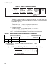
Table 13.1-2 Transfer Cycles and Transfer Rates Available for the Dedicated Baud Rate Generator
(when F
CH
= 12.5 MHz)
Transfer rate (µs/baud)
Clock divider = 2.5
(PR2=0, PR1=1, PR0=0)
Clock divider = 1
(PR2=0, PR1=0, PR0=0)
RC2 RC1 RC0
Divider for baud rate
(multiplier = n)
Asynchronous
transfer
Synchronous
transfer
Asynchronous
transfer
Synchronous
transfer
0 0 0 1(0) 83/12019 0.8/1.25M 33/30048 0.32/3.1M
0 0 1 2(1) 166/6010 1.6/625k 67/15024 0.64/1.6M
0 1 0 4(2) 333/3005 3.2/313k 133/7512 1.28/781k
0 1 1 8(3) 666/1503 6.4/156k 266/3756 2.56/391k
1 0 0 16(4) 1331/751 12.8/78k 532/1878 5.12/195k
1 0 1 32(5) 2662/375 25.6/39k 1065/939 10.24/98k
1 1 0 2(1) 13/78125 1.6/625k 5.12/195k 0.64/1.6M
1 1 1 16(4) 102/9766 12.8/78k 41/24k 5.12/195k