


261
CHAPTER 12 A/D CONVERTER
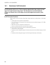
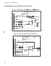
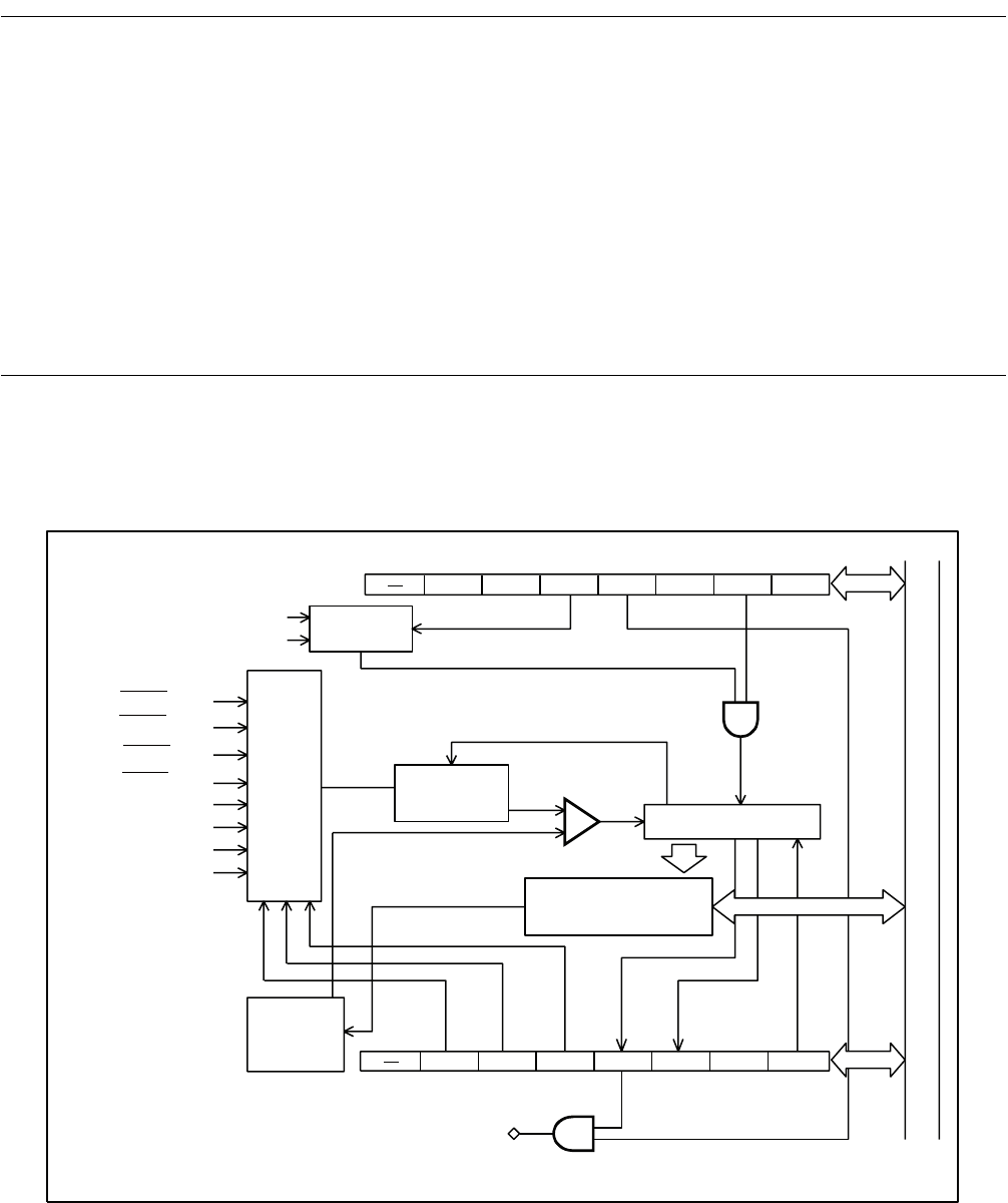
12.2 Configuration of A/D Converter
The A/D converter consists of the following nine blocks.
• Clock selector (input clock selector for activation of A/D conversion)
• Analog channel selector
• Sample hold circuit
• D/A converter
• Comparator
• Control circuit
• A/D data register (ADDH and ADDL)
• A/D control register 1 (ADC1)
• A/D control register 2 (ADC2)
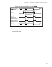
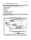
■ Block Diagram of the A/D Converter
Figure 12.2-1 Block Diagram of the A/D Converter
RESV4
RESV3
ADCK ADIE RESV2 EXT
RESV1
ANS2ANS1ANS0
ADI
ADMV RESV0
AD
TO
F
CH
(ADDH,ADDL)
IRQ8
A/D control register 2 (ADC2)
TO
(output of an 8/16-bit timer)
(output of a time-base
timer)
2
8
/F
CH
Clock
selector
Analog
channel
selector
Sample
hold
circuit
Comparator
Control circuit
Internal data bus
A/D data register
D/A
converter
A/D control register 1 (ADC1)
: Output of an 8/16-bit capture timer/counter
: Oscillation
P03/INT23/AN7
P02/INT22/AN6
P01/INT21/AN5
P00/INT20/AN4
P43/AN3
P42/AN2
P41/AN1
P40/AN0