


247
CHAPTER 11 EXTERNAL INTERRUPT CIRCUIT 2 (LEVEL)
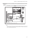
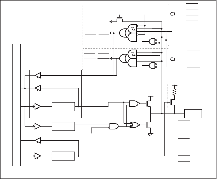
■
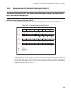
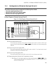
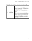
Block Diagram of Circuitry Terminating at the Pins Associated with External Interrupt
Circuit 2
Figure 11.3-1 Block Diagram of Circuitry Terminating at the Pins Associated with External Interrupt
Circuit 2
Note:
When the ON setting of the pull-up resistor is selected by the pull-up setting register, the pin state will
be "H" level (pull-up state) rather than Hi-Z during stop mode (SPL = 1). During a reset, however, the
pull-up is invalid and the pin remains at Hi-Z.
DDR
P-ch
N-ch
PDR
PUL
Internal data bus
PDR read
PDR read
(when read-modify-write
is performed)
Output
latch
PDR write
DDR write
PUL read
PUL write
To A/D
converter's
analog input
A/D converter
channel select
A/D converter
enable bit
From external
interrupt enable
Stop mode
(SPL = 1)
Stop mode
(SPL = 1)
Pull-up
resistor
Pins
SPL: Pin status setting bit of standby control register (STBC)
P00/INT20/AN4
P01/INT21/AN5
P02/INT22/AN6
P03/INT23/AN7
INT20, INT21
INT22, INT23
INT24, INT25
INT26, INT27
P04/INT24
P05/INT25
P06/INT26
P07/INT27
P00/INT20/AN4
P01/INT21/AN5
P02/INT22/AN6
P03/INT23/AN7
P04/INT24
P05/INT25
P06/INT26
P07/INT27