


358
CHAPTER 17 FLASH MEMORY
17.1 Overview of Flash Memory
The 128K-bit flash memory is mapped to the C000
H
to FFFF
H
bank in the CPU memory
map. The functions of the flash memory interface circuit enable read-access and
program-access from the CPU in the same way as mask ROM. Instructions from the
CPU can be used via the flash memory interface circuit to write data to and erase data
from the flash memory. Internal CPU control therefore enables rewriting of the flash
memory while it is mounted. As a result, improvements in programs and data can be
performed efficiently.
■ Flash Memory Features
• 16 Kbyte × 8-bit configuration
• Use of automatic program algorithm (Embedded Algorthm)
• Detection of completion of writing/erasing using data polling or toggle bit functions
• Detection of completion of writing/erasing using CPU interrupts
• Compatible with JEDEC standard commands
• Minimum of 10000 write / erase operations (MB89F202/F202RA)
■
High voltage supply on RST pin (applicable to MB89F202RA only)
During writing data to or erasing all data in flash memory, a typical +10V D.C. voltage should be applied at
the RST pin. After applying the high voltage, wait for 10ms before writing data or erasing all data in flash
memory. And this applied voltage should be kept at the RST
pin until data writing or erasing has been
completed.
■
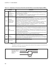
Writing to/Erasing Flash Memory
The flash memory cannot be written to and read at the same time. That is, when data is written to or erased
data from the flash memory, the program in the flash memory must first be copied to RAM. The entire
process is then executed in RAM so that data is simply written to the flash memory. This eliminates the
need for the program to access the flash memory from the flash memory itself.
■
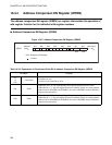
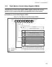
Flash Memory Register
Compatible with JEDEC standard commands
Bit No. bit7 bit6 bit5 bit4 bit3 bit2 bit1 bit0
0079
H
INTE RDYINT WE RDY - - - -
Read/write (R/W) (R/W) (R/W) (R) (-) (-) (-) (-)
Initial value (0) (0) (0) (X) (-) (-) (-) (-)