


270
CHAPTER 12 A/D CONVERTER
12.4.3 A/D Data Register (ADDH and ADDL)
A/D data register (ADDH and ADDL) stores the results of A/D conversion at 10-bit A/D
conversion.
The high-order 2 bits of 10-bit data correspond to the ADDH register. The low-order 8
bits correspond to the ADDL register.
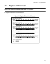
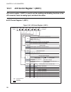
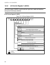
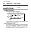
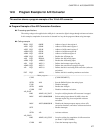
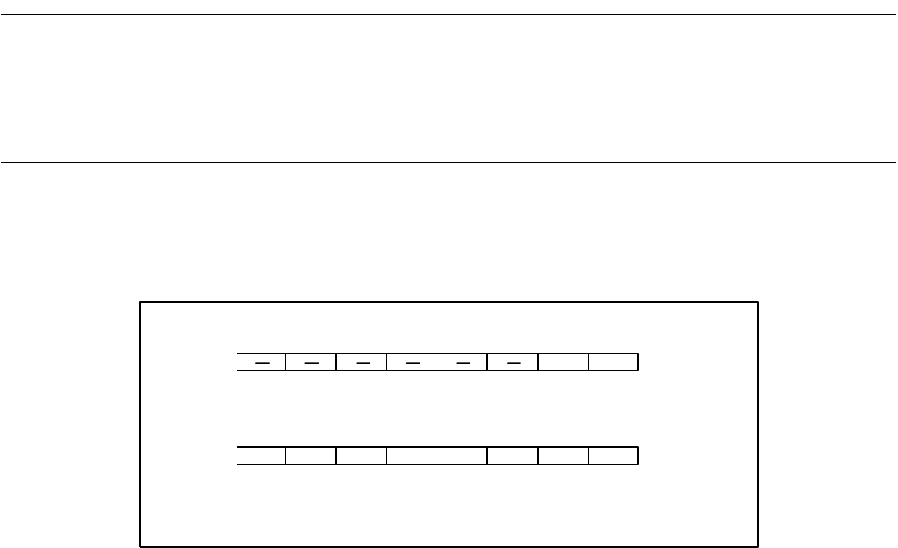
■ A/D Data Register (ADDH and ADDL)
Figure 12.4-4 shows the bit configuration of the A/D data registers.
Figure 12.4-4 A/D Data Registers (ADDH and ADDL)
Of the 10-bit A/D data, the high-order 2 bits correspond to bits 1 and 0 in the ADDH register. The low-
order 8 bits correspond to bits 7 to 0 in the ADDL register.
● When A/D conversion functions are enabled
When A/D conversion is activated, after about 38 instruction cycles, the data on the conversion results are
fixed and stored to these registers. Therefore, after A/D conversion, read these registers (conversion
results), write "0" to the ADI bit (bit3) in the ADC1 register until the next A/D conversion is completed,
and clear the flags after A/D conversion. During A/D conversion, the values in these registers are not
determined. When A/D conversion functions are enabled, these registers function as read-only registers.
bit7 bit6 bit5 bit4 bit3 bit2 bit1 bit0
0032
H
------XX
B
RR
bit7 bit6 bit5 bit4 bit3 bit2 bit1 bit0
0033
H
XXXXXXXX
B
RRRRRRRR
R : Read only
X : Undefined
ADDH (A/D data register H)
Address Initial value
ADDL (A/D data register L)
Address
Initial value