109
CHAPTER 4 I/O PORTS
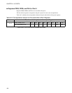
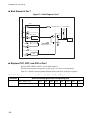
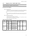
4.7.1 Registers of Port 7 (PDR7, DDR7, PUL7)
This section describes the registers associated with port 7.
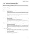
■ Functions of Port 7 Registers
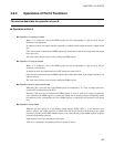
● Port 7 data register (PDR7)
The PDR7 register indicates the state of the output latch. For a pin set to function as an output port, the
same value ("0" or "1") as the value state of the output pin can be read from this register. If the pin is set
to function as an input port, however, its output latch value cannot be read from the register.
Note:
When a bit manipulation instruction (SETB, CLRB) is executed, the output latch values, not the value
states of the pins, are read; thus, output latch values, other than those for bits to be manipulated, do not
change.
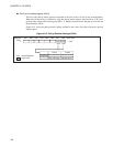
● Port 7 data direction register (DDR7)
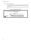
The DDR7 register sets the I/O direction of each pin per bit.
When a bit of the DDR7 corresponding to a pin of port 7 is set to "1", the pin functions as an output
port. When the bit is set to "0", the pin functions as an input port.
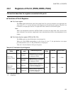
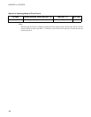
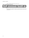
Table 4.7-3 lists the functions of the port 7 registers.
Table 4.7-3 Functions of Port 7 Registers
Register
name
Data
When being
read
When being written
Read/
Write
Address Initial value
Port 7 data
register (PDR7)
0
Pin state is
"L" level.
Output latch of "0" is set and
"L" level is output to the pin
in output port mode.
R/W 0063
H
-----XXX
B
1
Pin state is
"H" level.
Output latch of "1" is set and
"H" level is output to the pin
in output port mode.
Port 7 data
direction
register (DDR7)
0 Input port
Output transistor operation
is disabled and the pin is set
to serve as an input pin.
R/W 0064
H
-----000
B
1 Output port
Output transistor operation
is enabled and the pin is set
to serve as output pin.
R/W : Readable and Writable
X : Undefined


