


12
CHAPTER 1 OVERVIEW
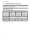
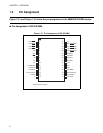
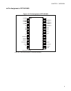
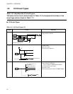
1.7 Pin Functions Description
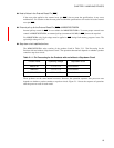
Table 1.7-1 describes the I/O pins and functions.
The letters in the circuit type column shown in Table 1.7-1 correspond to the letters in
the Circuit Type column shown in Table 1.8-1 .
■ Pin Functions Description
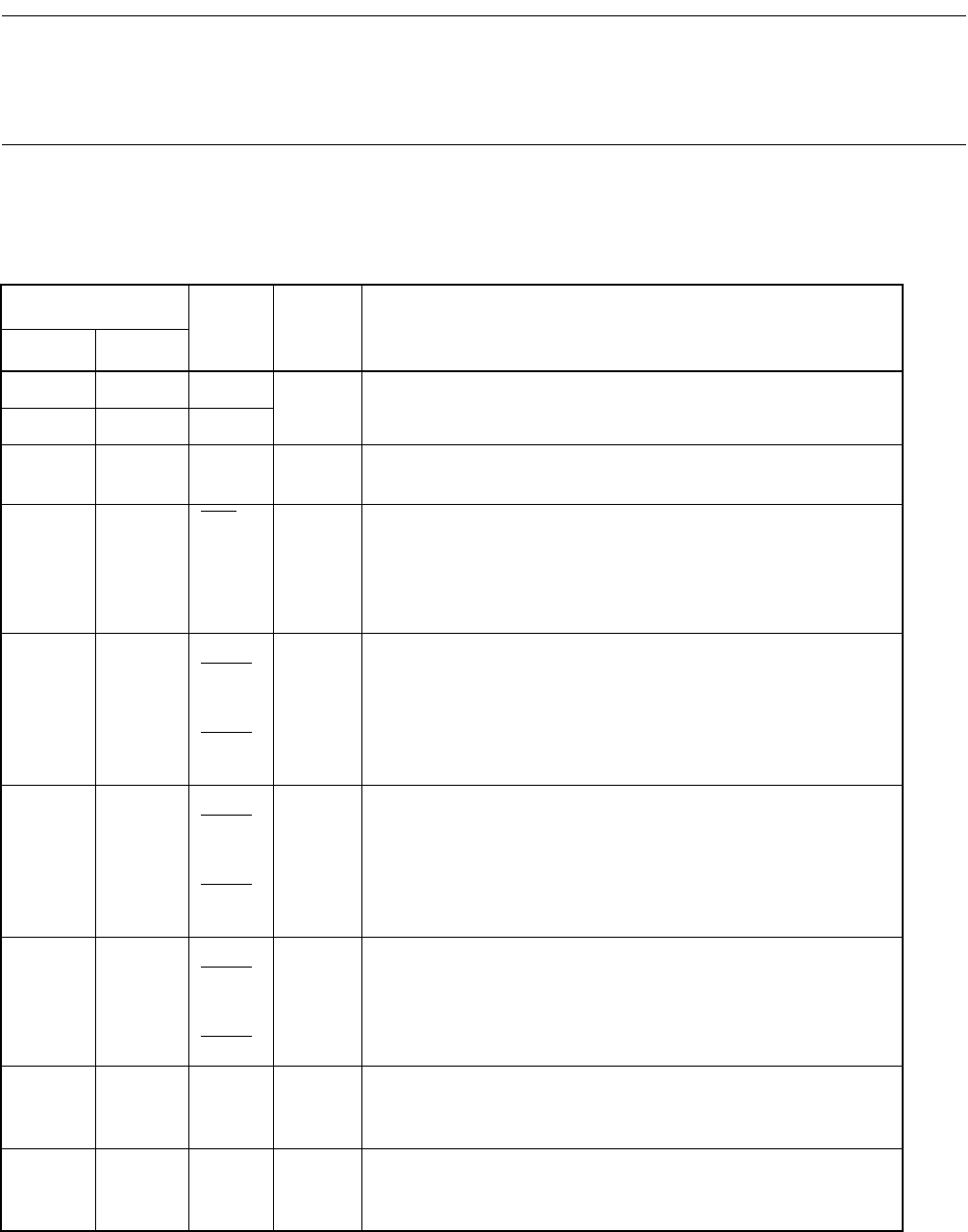
Table 1.7-1 Pin Functions Description (1/2)
Pin No.
Pin
name
Circuit
type
Function
SHDIP32
*1
SSOP34
*2
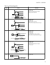
8 8 X0 A Pins for connecting the crystal for the main clock. To use an
external clock, input the signal to X0 and leave X1 open.
99X1
5, 6 5, 6 P60,
P61
H / E General-purpose CMOS input port.
77RST
C Reset I/O pin.
This pin serves as an N-ch open-drain reset output and a reset input
as well. The reset is a hysteresis input.
It outputs the "L" signal in response to an internal reset request.
Also, it initializes the internal circuit upon input of the "L" signal.
28, 29 30, 31 P00/
INT20
/
AN4,
P01/
INT21
/
AN5
G General-purpose CMOS I/O ports.
These pins also serve as an input (wake-up input) of external
interrupt 2 or as an 10-bit A/D converter analog input. The input of
external interrupt 2 is a hysteresis input.
30, 31 32, 33 P02/
INT22
/
AN6,
P03/
INT23
/
AN7
G General-purpose CMOS I/O ports.
These pins also serve as an input (wake-up input) of external
interrupt 2 or as an 10-bit A/D converter analog input. The input of
external interrupt 2 is a hysteresis input.
1 to 4 1 to 4 P04/
INT24
to
P07/
INT27
D General-purpose CMOS I/O ports.
These pins also serve as an input (wake-up input) of external
interrupt 2. The input of external interrupt 2 is a hysteresis input.
19 20 P30/
UCK/
SCK
B General-purpose CMOS I/O ports.
This pin also serves as the clock I/O pin for the UART or 8-bit
serial I/O. The resource is a hysteresis input.
18 19 P31/
UO/SO
E General-purpose CMOS I/O ports.
This pin also serves as the data output pin for the UART or 8-bit
serial I/O.