


November 2003 © TOSHIBA TEC 6 - 11 e-STUDIO3511/4511 SCANNER
6
6.5 General Description of CCD Control
6.5.1 Opto-electronic conversion
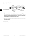
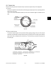
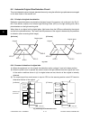
A CCD (Charge-Coupled Device) is used to produce electrical signal corresponding to the reflected light
amount from the original. CCD is a one-chip opto-electronic conversion device, comprised of several
thousand light-receiving elements arranged in a line, each one of them is a few micron square.
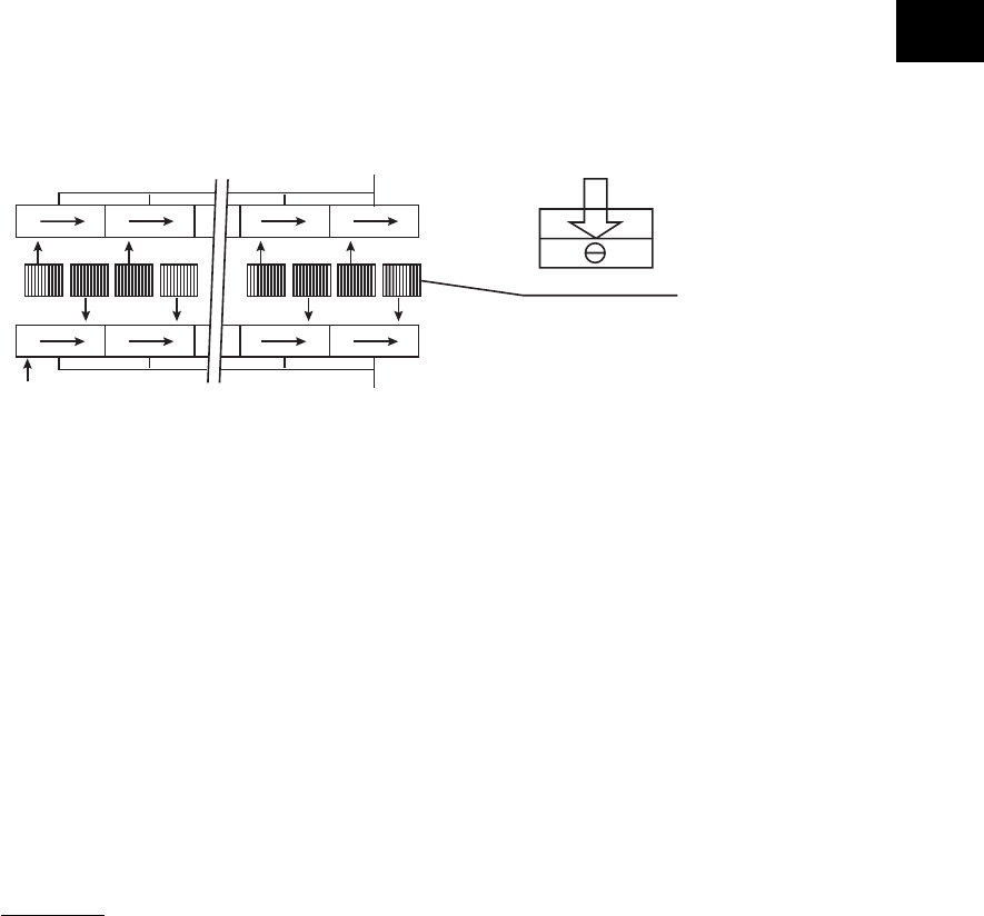
This equipment includes a CCD which has 7,450 light-receiving elements.
Each element of the light-receiving section consists of semiconductive layers P and N. When the light
irradiates the element, light energy produces a (-) charge in the layer P; the amount of the charge
produced is proportional to the energy and irradiating time. The charges produced in the light-receiving
section are then sent to the transfer section where they are shifted by transfer clock from left to right as
shown in the figure below, and are finally output from the CCD. At this time, to increase the transfer
speed of the CCD, image signals in the even-number and odd-number elements are separated and
output in parallel via two channels.
1
7447 7448 7449 7450
2
34
Transfer section
Light receiving section
Transfer section
Shift register
Transfer clock
Light energy
layer N
layer P
Details of light receiving element
Transfer clock
Fig. 6-501
6.5.2 Shading correction
Signal voltages read by the CCD have the following characteristics:
(1) Light source has a variation in its light distribution.
(2) Since the light beam reflected from the original is converged using a lens, the light path is the
shortest at the center of the CCD and the longest at ends. This causes difference in the amount
of light reaching the CCD (i.e. the light amount is maximum at the CCD center, gradually decreases
toward ends).
(3) Each of the 7,450 elements varies in opto-electronic conversion efficiency.
These variation need to be corrected and this correction is referred to as shading correction. Shading
correction is performed by applying normalization process using the following formula on the black and
white data obtained in advance to correct lighting variance and element variation of the image data.
I = k x
(S — K)
(W — K)
k : Coefficient
S : Image data before correction
K : Black data (stored in “black” memory)
W : White data (stored in “white” memory)