


November 2003 © TOSHIBA TEC 3 - 3 e-STUDIO3511/4511 COPY PROCESS
3
3.3 Details of Copying Process
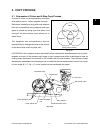
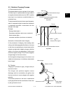
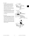
(1) Photoconductive drum
The photoconductive drum consists of two layers.
The outer layer is a photoconductive layer made of
an organic photoconductive carrier (OPC), and the
inner layer is an aluminum conductive base in a
cylindrical form.
The photoconductive carrier has a special property:
when it is exposed to light, the electrical resistance
it possesses increases or decreases with the
strength of the light.
Example:
· Strong incident light→
Decreases resistance (works as a conductor.)
· Weak incident light→
Increases resistance (works as an insulator.)
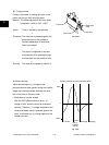
[Formation of electrostatic latent images]
In the processes of charging, data reading, data
writing, and discharging described below, the areas
on the drum corresponding to colored areas on the
original are deprived of negative charge, while the
areas on the drum corresponding to white areas
retain the negative charge. Thus it forms a negative
charge image on the drum surface.
As this negative charge image on the drum is not
visible to the human eye, it is called an “electrostatic
latent image.”
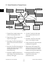
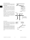
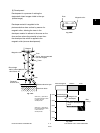
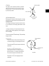
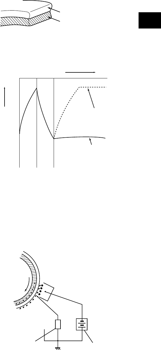
(2) Charging
Charging is a process to apply charge evenly to
the drum surface.
The charger wire produces negative corona
discharge, which is controlled by the grid so that
the drum surface is evenly charged with negative
potential.
The surface potential on the drum is determined
by the grid potential and is controlled to a fixed value
by the grid control circuit.
0
- 500
- 1000
Photoconductive layer
Base
Structure of the photoconductive drum
(Example of OPC)
Time (t)
Colored area of original
White area of original
Surface potential (V)
Discharge
process
Charging
process
Electric potential of the photoconductive drum
Main charger
Rotation of drum
Grid control circuit
High-voltage
transformer
Fig. 3-301
Fig. 3-302
Fig. 3-303