


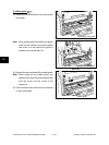
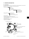
e-STUDIO3511/4511 DRUM RELATED SECTION 11 - 4 November 2003 © TOSHIBA TEC
11
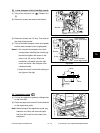
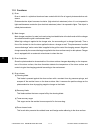
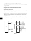
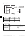
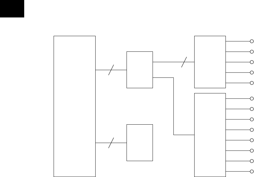
Fig. 11-301
11.3 Output Control Circuits of High-Voltage Transformer
• Outputs adjustment value of the main charger, transfer charger, and developer biases in the NVRAM
to the main processor.
↓
• Outputs control voltage data from the main processor to the D/A converter.
↓
• Analog conversion by the D/A converter.
↓
• Outputs control voltage Vc to the main charger grid bias, 1st transfer roller bias, 2nd transfer roller
bias, color developer bias and black developer bias transformer.
↓
• The main charger bias, 1st transfer roller bias, 2nd transfer roller bias, color developer bias and black
developer bias transformers generate output current or voltage proportional to the control voltage Vc
with the output ON signal.
* Adjustment of the control voltage Vc (change of adjustment data) is performed in the Adjustment
Mode (05).
* Output value of the cleaning blade bias is fixed when the transformer board is shipped from the
factory.
MAIN
CPU
NVRAM
Main charger grid
1st transfer
2nd transfer
Black developer
Color developer
Main charger ON
1st transfer
2nd transfer
Black developer
(
DC
) ON
Black developer
(
AC
) ON
Cleaning blade ON
Color developer
(
DC
) ON
Color developer
(
AC
) ON
D/A
converter
IC8
Transistor
array
IC7
Gate
array
IC29
IC34