


November 2003 © TOSHIBA TEC 12 - 15 e-STUDIO3511/4511 DEVELOPER UNIT
12
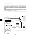
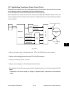
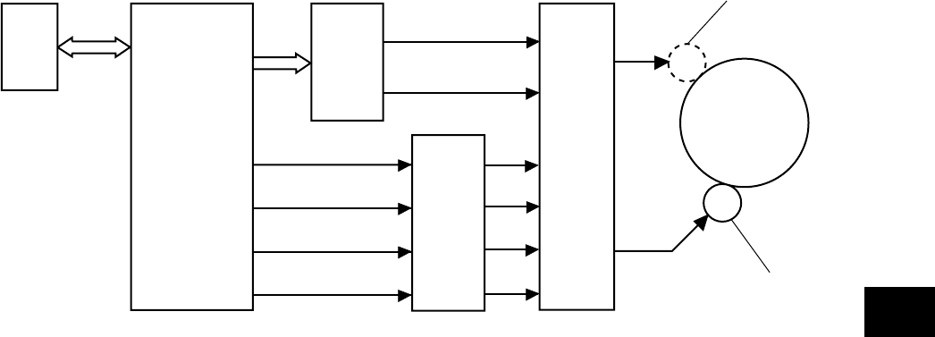
12.7 High-Voltage Transformer Output Control Circuit
Developer bias is supplied from high-voltage power supply to the developer sleeve and the toner image
on the developer sleeve is transferred onto the photoconductive drum.
A color developer bias and a black developer bias are output separately.
Each developer bias consists of DC and AC which has an independent ON/OFF control. At DC, D/A
converter adjusts the level of output value in both color and black modes since each mode has a different
control condition.
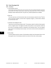
Fig. 12-701
• Outputs adjustment value of the developer bias (DC) in the NVRAM to the main processor.
↓
• Outputs control voltage data from the main CPU to the D/A converter.
↓
• Analog conversion by the D/A converter.
↓
• Outputs control voltage Vc to the developer bias transformer.
↓
• The developer bias transformer generates output voltage proportional to the control voltage Vc by ON-
signed.
* Adjustment of the control voltage Vc (change of adjustment data) is performed in the adjustment
mode.
CPU
LCA301-2
KDVDON-0
KVDAON-0
CDVDON-0
CDVAON-0
KDVVR
CDVVR
PWA-HVT
Gate array
Buffer
Black developer
sleeve
Photoconductive
drum
Color developer sleeve
D/A
converter