


e-STUDIO3511/4511 OUTLINE OF THE MACHINE 2 - 22 November 2003 © TOSHIBA TEC
2
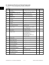
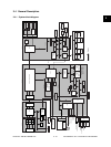
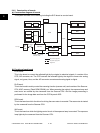
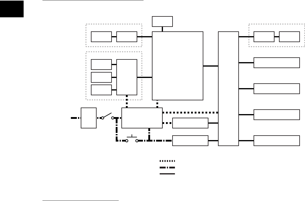
2.4.2 Construction of boards
(a) Construction diagram of boards
This system consists of the following including the SYS board as a main board.
:
DC power supply line
:
AC power supply line
:
Signal line
AC input
Main switch
Cover opening/closing
interlock switch
SYS
PS-ACC
FIL
or
FUS
LGC
CCD
SDV
INV
SLG
Scanner unit
KEY
DSP
Control panel
NIC
ADU
SFB
CCL
HVT
DRV
IH
LDR
SNS
Laser unit
(b) Function of each board
CCD board:
This is the board to convert the reflected light by the original to electrical signals. It consists of the
CCD, A/D converter, etc. The CCD converts the reflected light by the original to three-color analog
signal; red, green, blue, and the A/D converter converts each analog signal to digital.
SLG board:
This is the board to mainly control the scanning function (scanner unit) and consists of the Scanner-
CPU, ASIC, memory (Flash ROM, SRAM), etc. When scanning the original, the exposure lamp and
scan motor are started by the command from the Scanner-CPU. And the image processing is
performed for the image data sent from the CCD by each ASIC.
SDV board:
This is the board on which the driver for driving the scan motor is mounted. The scan motor is started
by the command from the Scanner-CPU.
INV board:
This is the board on which the lighting control circuit of the exposure lamp is mounted. The exposure
lamp lights by the command from the Scanner-CPU.