


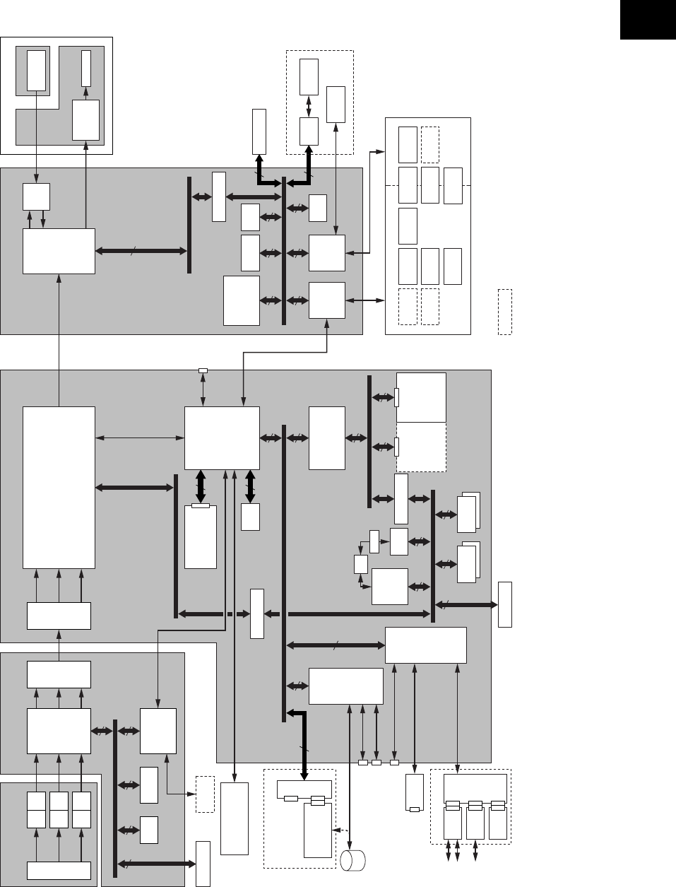
November 2003 © TOSHIBA TEC 2 - 21 e-STUDIO3511/4511 OUTLINE OF THE MACHINE
2
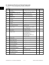
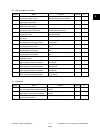
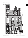
2.4 General Description
2.4.1 System block diagram
LGCSYSSLGCCD
SNS
Laser unit
LDR
8
8
16
8
888
16
8
64
64 64
16
8
32
32
8
32 16
32 32
32
3232
32
8
16168
PSTN
External TEL
PSTN
PCI-bus
Data-bus
Data-bus
Data-bus
Data-bus
Data-bus
Laser beam
sensor
ASIC
PWM
ASIC
ASIC
System CPU
333MHz
Image processing
(
ASIC
)
Engine CPU
24MHz
Gate array
#2
ASIC
ASIC
ASIC
Gate array
#1
SRAM
128KB
SRAM
512KB
NVRAM
8KB
NVRAM
256KB
Flash ROM
512KB
Flash ROM
2MB x 2
Battery
RTC
Flash ROM
4MB x 2
Laser diode
Download jig
Download jig
Download jig
IPC
PFP/LCF
RADF
ADU Motors
HVT Clutches Sensors Solenoids
Switches
Bypass
unit
Key counter
Copy key
card
Finisher
Bridge unit
Bus transceiver
Bus transceiver
Bus transceiver
I/O
Finisher
Page memory
(
DIMM
)
Standard
:
128MB
Option
:
256MB
Control panel
PCI external slot
Scrambler board
USB connector
(
device
)
USB connector
(
host
)
RS-232C
Parallel port
(
IEEE-1284
)
HDD
NCU
(
LINE-1
)
NCU
(
LINE-2
)
NIC
Modem
FAX
CCD
ASIC
LVD S
receiver
Scanner CPU
22MHz
Flash ROM
512KB
SRAM
128KB
Amp
Amp
Amp
A/D
A/D
A/D
LVD S
driver
FAX
Scrambler board
LAN connector
(
10BASE-T/100BASE-TX
)
: Option
(
R
)
(
G/K-odd
)
(
B/K-even
)
Main memory
(
DIMM
)
#0
Standard
:
Not installed
Option
:
128MB
*Main memory total
Standard
:
256MB x 1
Option
:
128MB x 2
Main memory
(
DIMM
)
#1
Standard
:
256MB
Option
:
128MB