CM71-00105-1E FUJITSU MICROELECTRONICS LIMITED 125
FR81 Family
CHAPTER 7 DETAILED EXECUTION INSTRUCTIONS
7.11
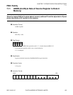
7.11 ANDB (And Byte Data of Source Register to Data in
Memory)
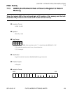
Takes the logical AND of the byte data at memory address Ri and the byte data in Rj and
stores the results at Ri location in the memory.
● Assembler Format
ANDB Rj,@Ri
● Operation
(Ri) & Rj → (Ri)
● Flag Change
N: Set when the MSB of the operation result is "1", cleared when the MSB is "0".
Z: Set when the operation result is zero, cleared otherwise.
V, C: Unchanged.
● Classification
Logical calculation instruction, Read/Modify/Write type instruction
● Execution Cycles
1+2a cycles
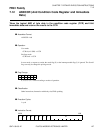
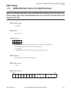
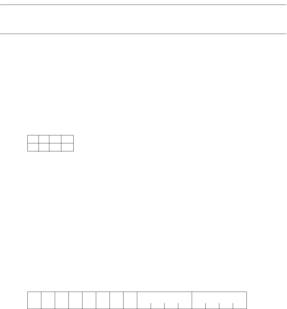
● Instruction Format
NZV C
CC - -
MSB LSB
10000110 Rj Ri


