


FR81 Family
10 FUJITSU MICROELECTRONICS LIMITED CM71-00105-1E
CHAPTER 2 MEMORY ARCHITECTURE
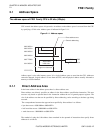
2.1
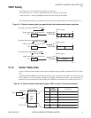
As a result of reset, the value of Table Base Register (TBR) is initialized to 000F FC00
H
, and the range of
vector table area extends from 000F FC00
H
to 000F FFFF
H
. By rewriting the Table Base Register (TBR),
the vector table area can be allocated to any desired location.
A vector table is composed of entry addresses for each EIT processing programs. Each vector table
contains values whose use is fixed according to the CPU architecture, and values that vary according to the
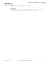
type of built-in peripheral functions. The structure of vector table area is shown in Table 2.1-1.
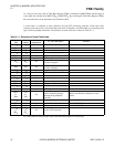
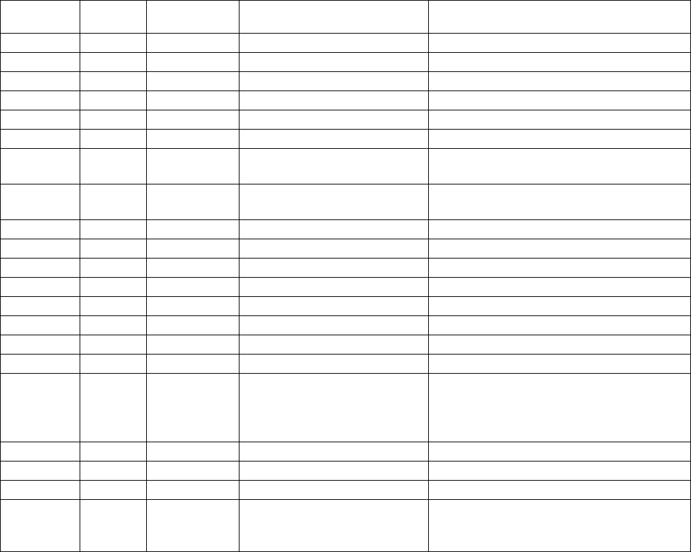
Table 2.1-1
Structure of Vector Table Area
For vector tables of actual models, refer to the hardware manuals for each model.
Offset from
TBR
Vector
number
Model-
dependence
EIT value description Remarks
3FC
H
00
H
No reset
3F8
H
01
H
No system reserved
3F4
H
02
H
No system reserved Disabled
3F0
H
03
H
No system reserved Disabled
3EC
H
04
H
No system reserved Disabled
3E8
H
05
H
No FPU exception
3E4
H
06
H
No
Instruction access protection
violation exception
3E0
H
07
H
No
Data access protection
violation exception
3DC
H
08
H
No Data access error interrupt
3D8
H
09
H
No INTE instruction For use in the emulator
3D4
H
0A
H
No Instruction break
3D0
H
0B
H
No system reserved
3CC
H
0C
H
No Step trace trap
3C8
H
0D
H
No system reserved
3C4
H
0E
H
No Invalid instruction exception
3C0
H
0F
H
No NMI request
3BC
H
to
304
H
0F
H
to
3E
H
Yes
General interrupt
(used in external interrupt,
interrupt from peripheral
function)
Refer to the Hardware Manual for each
model
300
H
3F
H
No General interrupts Used in Delayed interrupt
2FC
H
40
H
No system reserved Used in REALOS
2F8
H
41
H
No system reserved Used in REALOS
2F4
H
to
000
H
42
H
to
FF
H
No Used in INT instruction