CM71-00105-1E FUJITSU MICROELECTRONICS LIMITED 9
FR81 Family
CHAPTER 2 MEMORY ARCHITECTURE
2.1
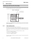
• byte data access: Lower 8 bits of the address are used as it is
• half word data access: Value is doubled and used as lower 9 bits of the address
• word data access: Value is quadrupled and used as lower 10 bits of the address
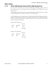
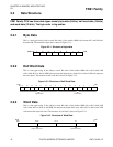
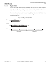
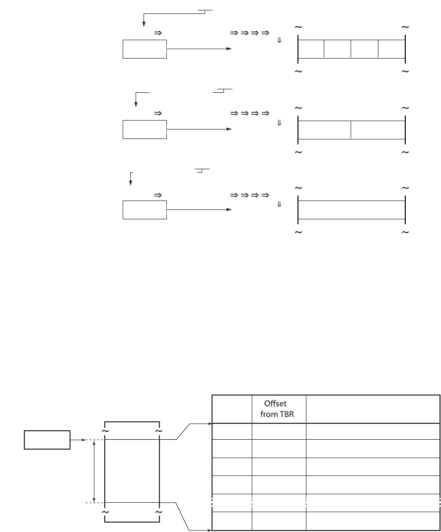
The relation between data types specified by direct address and memory address is shown in Figure 2.1-2.
Figure 2.1-2
Relation between data type specified by direct address and memory address
2.1.2 Vector Table Area
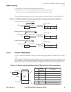
An area of 1Kbyte from the address shown in the Table Base Register (TBR) is called the EIT Vector Table
Area.
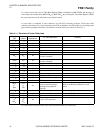
Table Base Register (TBR) represents the top address of the vector table area. In this vector table area, the
entry addresses of EIT processing (Exception processing, Interrupt processing, Trap processing) are
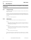
described. The relation between Table Base Register (TBR) and vector table area is shown in Figure 2.1-3.
Figure 2.1-3 Relation between Table Base Register (TBR) and Vector Table Area addresses
[Example 1] Byte data: DMOVB R13,@58H
[Example 2] Half-word data: DMOVH R13,@58H
[Example 3] Word data: DMOV R13,@58H
Object code:1A58H
0000 0058HR13 12345678
0000 0058
H
R13 12345678
0000 0058
HR13 12345678
Right 1-bit shift
Right 2-bit shift
Memory space
Memory space
Memory space
78
5678
1345678
58
H
No data shift
Object code:192C
H 58HLeft 1-bit shift
Object code:1816
H 58HLeft 2-bit shi
f
t
0000 0000H
FFFF FFFFH
TBR
1 Kbyte
Number
EIT source
FF
H
FEH
FDH
FCH
00H
000H
004H
008H
00CH
3FCH
Entry address for INT instruction
Entry address for INT instruction
Entry address for INT instruction
Entry address for INT instruction
Entry address for reset processing
Memory space
Vec t o r
table
area


