


5700A/5720A Series II Calibrator
Service Manual
2-44
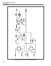
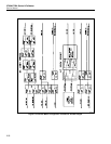
The Switch Matrix assembly consists of 33 latching type, two- and four-pole relays. The
relays are driven by special driver chips, which are controlled by the assembly’s 24-
output 82C55 chip. The Switch Matrix also contains the 5700A-4HR1 Temperature-
Controlled Precision DC Amplifier Hybrid and RNET assembly, which is used when the
calibrator is in the dc 2.2V or 220 mV range. The resistor network also is used to create
resistive dividers to generate the ac or dc 220 mV, ac 22 mV, and ac 2 mV ranges.
Additional analog circuitry in the Switch Matrix Assembly includes the dc 2.2V range
output stage, the internal cal zero amplifier, FETs to support assembly calibration,
assembly diagnostics, and circuitry to control some of the motherboard relays.
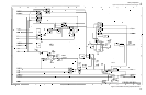
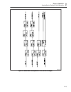
2-88. Switch Matrix Digital Control
Refer to sheet four of the Switch Matrix schematic diagram for the following discussion.
The heart of the Switch Matrix digital control circuitry is an 82C55 Programmable
Peripheral Interface IC (U1) under software control via the guarded digital bus. This IC
has three ports that generate 24 outputs. These outputs are used to control eight
UCN5801 Latching Driver ICs (U5-U12) controlling all Switch Matrix latching relays,
one UCN5801 Latching Driver (U13) controlling the 10 non-latching relays on the
motherboard, a 4028 decoder (U2), five FET switches (Q6-Q7, Q9-Q11), and an analog
multiplexer (U4) for self diagnostics.
Eight UCN5801 latching driver ICs (U5-U12) drive Switch Matrix latching relays. Port
A (PA0-PA7) from U1 provides a common input bus. Each driver chip has a separate
strobe line. A 4028 decoder (U2) generates strobe lines U5STB-U13STB for strobing
U5-U13 respectively. These individual strobe lines are decoded from PB0-PB3 of U1.
When a strobe line is selected, the data on the bus is strobed in the respective driver chip.
The output enables are controlled directly by PC0-PC3 of U1. One bit of port C enables
two drivers. PC0 enables U5 and U6, PC1 enables U7 and U8, PC2 enables U9 and U10,
and PC3 enables U11 and U12. By enabling only two driver ICs at a time, excessive
power supply current draw is prevented. To ensure that the relays are latched properly,
the driver chips must be enabled for 10 ms. As an example, the following steps are taken
to set up relays in the first bank:
1. Write the proper data for the relays associated with driver U5 (K2,K9, K11, and
K15) to port A of the 82C55.
2. Write 0 hex to PB0-PB3 to make U5STB go high. Now write 9 hex toPB0-PB3 to
make all strobe lines go low. The data has now been strobed into U5.
3. Write the proper data for the relays associated with U6 (K3, K4, K5, and K24) to
port A of the 82C55.
4. Write 1 hex to PB0-PB3 to make U6STB go high. Now write 9 hex toPB0-PB3 to
make all strobe lines go low. The data has now been strobed into U6.
5. Write FE hex to port C (PC0 is low), wait 10 ms and write FF hex to port C. This
takes the outputs of U5 and U6 out of tri-state and allows the proper relay coils to be
energized for 10 ms.