


5700A/5720A Series II Calibrator
Service Manual
2-82
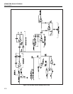
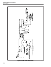
2-131. Oscillator Output Digital Control
The digital control circuit consists of an 82C55 Programmable Peripheral Interface
(U26), a 5801 Latching Relay Driver (U24), and three HC374 Octal D-Type Flip Flops
(U12, U32, U33). The Programmable Peripheral Interface (U26) is under software
control via the guarded digital bus and has three ports which generate 24 outputs. Port A
(PA0-PA7) is a common input bus for U24, U12, U32, U33, and U28. Latching relay
driver U24 controls the four latching relays K1-K4. Relays K1-K3 select the frequency
range and K4 selects the voltage range. This IC is strobed by PC3 of port C and enabled
by PC6 of port C. To ensure that the relays are latched properly the driver must be
enabled for 10 ms.
Latch U32 is clocked by PC0 and generates the data bus FREQ DATA for controlling 8-
bit resolution hybrid resistive dacs U5 and U7. Latch U12 is clocked by PC1 and
generates the data bus AMPL DATA for controlling U11, which is identical to U5 and
U7. Latch U33 is clocked by PC2 and generates control bus PHASE, which controls
multiplexer U27 in the phase shifter circuit and control bus MUX, which controls the
SDL multiplexer U25 in the diagnostic circuit. This diagnostic circuit monitors the ±44S
supplies, ±15S supplies, INTEGRATOR OUT, LOOP FILTER OUT, and AMP1 which
is from U30, the A13A1 assembly. These voltages are divided by Z2 and Z3 and
connected to the SDL line by multiplexer U25, where they are measured by the adc
circuit on the DAC assembly (A11).
PB0-PB2 of port B generates control bus PLOCK RNG which is used in the phase-
locked loop circuit. PB4 is control line 0/180 to control FET Q7 via comparator U31B in
the phase-locked loop circuit. PB6 is control line LFCOMP* to control FET Q6 via
comparator U20A in the integrator circuit. PB7 is control line HFCOMP*, which is
routed to the Oscillator Control assembly (A12). PC4 and PC5 are control lines DAC
STRB and DAC SEL respectively, which control the dual 8-bit dac U28 in the phase
shifter circuit. PC7 is control line INH to enable the multiplexer U25 in the diagnostic
circuit.
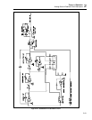
2-132. Quadrature RC Oscillator
The quadrature oscillator is a double integrator type. It contains two op amp RC
integrators and a unity-gain inverting summing amplifier. The integrators are identical
and use relay-switched feedback capacitors to select five frequency ranges. An 8-bit
resolution resistive dac selects frequency within a range.
The summing amplifier uses op amp U3 to provide a 180º phase shift in the oscillator
loop at unity gain. Its exact phase shift and gain are adjusted by the amplitude control
and phase-locked loop circuits to satisfy the conditions required for amplitude stable
oscillation: exactly 360º loop-phase and unity gain. This amplitude control circuit uses
an integrator and multiplier as outlined on sheet 1 of the schematic. These two circuits
are described in detail later.
The two op amp RC integrators are the quadrature amplifier and the oscillator amplifier.
Their purpose is to provide -90º each to the loop phase with an amplitude slope of -
20dB/decade. The quadrature amplifier contains op amp U6, 8-bit resolution resistive
dac U5, and relays K1B, K2B, and K3B. The relays select feedback capacitors C25, C24,
C22, and C21 for frequency ranges 100 Hz, 1 kHz, 10 kHz and 100 kHz respectively.
For the 1 MHz range, all the above capacitors are removed from the loop, and the only
feedback path is C19. The input resistor is the 8-bit resolution resistive dac U5 which is
under the control of the FREQ DATA bus from the digital control circuit. Its equivalent
resistance is R = (256/X)*2 kΩ, where X is the digital code on the FREQ DATA bus.
The oscillator amplifier contains op amp U9 and performs the same function as the
quadrature amplifier. Its input resistance is controlled by resistive dac U7. Relays K1A,
K2A, and K3A select the feedback capacitance. Since their phase shift is constant with