


5700A/5720A Series II Calibrator
Service Manual
2-142
sensor from damage by shunting its input and output to ground through the 200Ω
resistors R2 and R18.
The negative voltage at the output of U4A also turns off transistor Q1 and causes control
line U9 ENABLE to go high. This disables relay driver U9, which turns off all attenuator
relays (K4-K7) and output relay K8.
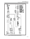
2-227. Wideband Output Digital Control
The heart of the Wideband Output assembly digital control circuitry is a 82C55
programmable peripheral interface IC (U7), which is under software control via the
guarded digital bus.
This IC has three ports, generating 24 outputs. These outputs control three relay drivers
(U6, U9, U10) and a 4051 analog multiplexer IC (U8) for self diagnostics.
Port A (PA0-PA7) is used as a common input bus for the relay drivers. Relay driver U6
controls latching relays K1, K2, K10, K11, and K12. Driver U6 is enabled by PC3 and
strobed by PC2. Relay driver U9 controls non-latching relays K4-K8. Driver U6 is
strobed by PC0 and enabled by control line U9 ENABLE, which is generated in the
overload control circuit. Relay driver U10 controls latching relays K3 and K9. It is
strobed by PC1 and enabled by PC3.
Relays K1 and K12 are controlled by the same drive lines and, when in the set position,
select the input from the Oscillator Output (A13) assembly during operation between 10
Hz and 1 MHz.
Relay K9 connects a 50Ω load (R43 and R44 in parallel) to the RCL line where the adc
circuit on the DAC assembly can monitor the output voltage and thereby determine
proper operation of the output attenuator resistors and relays.
The 4051 analog multiplexer IC (U8) is used by self-diagnostic routines for the
Wideband AC module. This allows the Calibrator to monitor three points on the
Wideband Output assembly and one point on the Wideband Oscillator assembly. Points
AMPLITUDE CONTROL, OUTPUT OFFSET, and SENSOR CAL are monitored on the
Wideband Output assembly, and point PLL DIAGNOSTIC is monitored on the
Wideband Oscillator assembly. PC4-PC6 of port C select which point the multiplexer
monitors. PC7 enables the output of U8 to the SDL line where is measured by the adc
circuit on the DAC assembly (A11).
2-228. Wideband Output Calibration
Linearity of the rms sensor is determined by configuring the Wideband Output similarly
to the second range of operation as described earlier. A difference is that the Oscillator
Output assembly operates at 1 kHz instead of between 12 kHz and 1.1 MHz during
operating in this range.
The Oscillator Output is set to 2.5V at 1 kHz. The resulting dc voltage from the rms
sensor is connected to the RCL line by relay K10 in the set position. The RCL line is
routed to the +input of the adc circuit on the DAC assembly, and the adc -input is
connected to the DAC output. The difference between the two is measured and stored in
memory. The Oscillator Output is increased to 7.0V and the difference between the two
adc inputs is again measured. Software uses these values to determine the linearity of the
rms sensor.
The previously calibrated 6.5V reference BRF6 and its sense line BSRF6, from the DAC
assembly is used to calibrate the 10 dB, 20 dB, and 40 dB attenuators.
Relays K3 A and B and K12 are in the set position. This connects the 6.5V reference to
the unity-gain amplifier and the attenuators. Output at the WIDEBAND Type "N"