


5700A/5720A Series II Calibrator
Service Manual
2-102
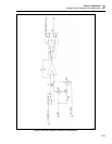
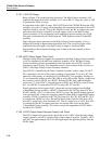
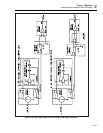
Resistor network Z5 and hybrid H4 determine the performance of the 2.2A range.
Current from the A7 assembly develops a voltage across the 57W portion of Z5. The
2.2A current amplifier circuit forces the same voltage across the 0.57W portion of Z5.
Because the ratio of these resistors is 100, the current through 0.57W resistor is 100
times that coming from the Current assembly (A7). Relay K12 connects this 2.2A range
current to B CUR where it is routed to the Current assembly (A7), which provides the
proper relay switching to the front panel binding posts.
The 2.2A amplifier circuit contains the heater-controlled hybrid H4, op amps U3-U5,
and transistors Q11-Q16. This circuitry is outlined as detail 2 on sheet 2 of the High
Voltage/High Current assembly schematic. The H4 hybrid consists of an op amp
mounted on a heated substrate. The heater control circuit adjusts the base voltage of Q18
to deliver the proper power to the heater resistor. This maintains the hybrid at a constant
temperature in spite of environmental temperature variations. Transistor Q19 protects the
hybrid in case Q18 fails.
The output of the H4 hybrid is a voltage directly proportional to the current output G
OUT. Q22 and R72-R76 form a high-frequency path for loop stability. In the ac current
function, op amp U3A and its associated circuitry create a half-wave signal equal to the
positive peaks of the ac signal from H4. Resistor R47 keeps this half-wave signal
approximately 0.7V above 0V. This half-wave signal is then subtracted from the ac
signal coming from H4 by op amp U3B and its associated circuitry. This creates a half-
wave signal equal to the negative peaks of the ac signal from H4. Resistor R45 keeps this
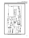
half-wave signal approximately 0.7V below 0V. Transistor Q15 and resistor R50
generate a current from the negative peaks created by U3B. Transistor Q16 and R48
generate a current from the positive peaks created from U3A. The current from Q15 and
R50 develops a voltage across the 191Ω resistor (R69). This voltage is used by op amp
U4 which drives transistors Q11 and Q12 in the Darlington configuration for current
gain. Resistor R67 is the feedback path for U4. The voltage across 191Ω resistor R69 is
the same as across the 0.1Ω resistors R68 and R78. Since the value of R68 and R78 is
1000 times less than R69, the current through R68 is 1000 times greater. The current
from Q16 and R48 is increased by 1000, in the same manner as previously stated, with
op amp U5, resistors R56, R57, and R77, and Darlington-configured transistors Q13 and
Q14.
Only half of the circuitry is used, since the output current is either positive or negative in
the dc current function. When outputting a positive current, the voltage from H4 is
negative. Since there is no positive voltage, the output of U3A is zero, thus no current is
developed by R48 and Q16. At this time, the negative voltage from U3B generates an
output current in the same manner as in the ac current function. The opposite occurs
when outputting a negative dc current.
2-162. 2
.
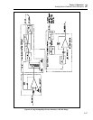
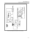
2A Power Supply Filter Circuit
The 2A range power supply filter circuit on the High Voltage Control assembly (A14),
operating in conjunction with the Power Amplifier assembly (A16), generates the VI
±supplies used by the 2.2A amplifier circuit on the High Voltage/High Current assembly
(A15). The High Voltage Control assembly generates an amplitude controlled square
wave, HVCL, from the square wave generator and square wave amplifier circuits. This
HVCL is amplified by the Power Amplifier assembly (A16), which is set for a gain of
10. This amplified output, PA OUT DC, is connected to the primary side of transformer
T1 by relay K1. The stepped-down secondary voltage is full-wave rectified by CR5 and
filtered by C3 and C4 to generate the VI+ and VI- supplies respectively. VI± are low-
voltage, high current supplies. These supplies, along with the secondary center tap VI
COM, are routed to the High Voltage assembly.