


5700A/5720A Series II Calibrator
Service Manual
2-46
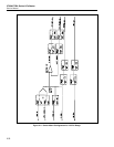
A UCN5801 driver (U13) drives non-latching relays on the motherboard. The
motherboard non-latching relay supply circuit, as outlined in sections A6 through A8 of
the schematic diagram, contains U17, Q1, Q2, CR1, CR2, CR10, and R6-R12. Port A of
U1 provides data for this driver (PA0-PA7), and decoder U2 provides the strobe signal.
Since this driver controls non-latching relays, the enable is tied to LH COM.
The non-latching relay supply circuit provides approximately 7V to the relays on the
motherboard during pull-in, and approximately 3.5V during normal operation. This
voltage is routed to the motherboard on the RLY+V line. The 7V is needed to ensure
pull-in while the 3.5V is sufficient to prevent drop out. This cuts relay heating and
thermal EMFs. PC5 controls the non-inverting amplifier U17. This amplifier is the
control element for Transistor Q1. When PC5 is low, the output is 3.5V, and when PB5
is high, the output is 7V. Components CR1, Q2 and R10-12 form a fold back current
limit for the supply. The following steps are taken to select a particular state for
Motherboard relays RLY1-RLY10:
1. Write the data corresponding to the desired state to port A(PA0-PA7) of the 82C55
(U1).
2. Strobe the data into U13 by writing 8 hex to PB0-PB3 to make U13STB go high,
then a 9 hex to make it go low.
3. Apply 7V to the relay coils by setting PC5 high.
4. Wait approximately 20 ms for the relays to pull in, then reduce the coil voltage to
3.5V by setting PC5 low.
There are five FETs on the Switch Matrix. Q9 and Q10 (sheet 3, C7), which are N-
channel JFETs controlled by port B (PB5) of U1, are driven by an LM393 open-collector
comparator (U15A) to provide the proper level shifting. DMOS enhancement FETs are
used for the remaining three FETs (Q6, Q7, and Q11). Refer to sheet 1, B5 of the
schematic diagram. FETs Q6 and Q7 are driven by U1, port B, with a high on PB4
turning on Q6, and a logic high on PB7 turning on Q7. FET Q11 is driven on by a logic
high from U1, port C (PC4).
The diagnostic circuit (sheet 4, B7) enables the calibrator to monitor +8RLH, the 2.2V
range output voltage, +5RLH, -5LH, +17S, -17S, the assembly temperature (U3), and the
OVEN TEMP line from the heated hybrid. OVEN TEMP, +5RLH, -5LH, and +8RLH
are divided down by a factor of 11 by Z5 and Z6. A 4051 analog multiplexer (U4) is
controlled by PA0-PA2 and PC6 from U1. This multiplexer selects which one of these
eight voltages is applied to the SDL line, where it is measured by the adc circuit on the
DAC assembly (A11).
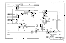
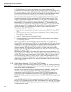
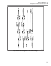
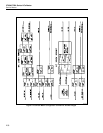
2-89. Switch Matrix Operation
:
11V DC and 22V DC Ranges
Refer to Figure 2-8 for the following discussion. DC 11V and 22V ranges are generated
by the DAC assembly and routed directly to the front panel binding posts through relays
on the Switch Matrix and Motherboard.
Line DAC HI is connected to INT OUT HI through relays K18B, K27, and K30. INT
OUT HI is connected to the OUTPUT HI binding post through relay K1 on the
motherboard. Line DAC SENSE HI is connected to INT SENSE HI through relays
K18A, K25, and K26. Motherboard relays K2 and K3 switch INT SENSE HI to the
SENSE HI binding post during external sensing, or OUTPUT/SENSE HI during internal
sensing.
Lines PA COM and DAC LO are connected by relays K11 and K12, and connected to
the OUTPUT LO binding post by relay K10. Switch Matrix relays K14 and K15 connect
R COM to the SENSE LO binding post during external sensing, or to OUTPUT/SENSE
LO during internal sensing.