Theory of Operation
Digital Section Detailed Circuit Description
2
2-31
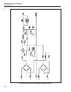
Output display filament driver circuitry consists of transistors Q7-Q12 and zener diodes
VR3 and VR4, plus associated resistors. The transistors are driven by 7406 open-
collector drivers U13C and U13D. These drivers are controlled by AOUT and BOUT as
in the Control Display. When AOUT is high, U13C turns Q8 and Q10 on. Q10 turns Q12
on, providing a path for the filament current through Q8 and Q12. Zener diode VR4
provides the dc voltage offset necessary for proper filament operation. Then when
BOUT is high, U13D turns Q7 and Q9 on. Q7 turns Q11 on, providing a path for the
filament current through Q9 and Q11, effectively reversing the direction of the voltage
driving the filament. Zener diode VR3 provides the dc voltage offset necessary for
proper filament operation.
Dual-port RAM U2 contains all the Output Display data written by the 68HC000
microprocessor on the CPU board. U5 contains a 7-bit address counter which U5 uses to
read the contents of U2. U2 provides a BUSYO signal to U3, which is active low
whenever the CPU and U5 try to access the same RAM location at the same time. If the
microprocessor attempts to write to the same RAM location U5 is reading as it refreshes
the Control Display, U3 uses BUSYO to hold off DTACK to the microprocessor. This
prevents written data from being lost. The other busy signal, generated when U5
attempts to read from a location being written to by the microprocessor, is ignored.
Losing display data for one refresh cycle is insignificant.
IC U5 also generates the FPINTR* (front panel interrupt, active low) signal sent to the
68HC000 microprocessor, telling it there is an encoder or keyboard interrupt. The
interrupt inputs to U5, ENCODERINTR (encoder interrupt, active high) and
KEYBOARDINTR (keyboard interrupt, active high), are generated by PLDs U24 and
U9 respectively.
2-52. Keyboard Scanner Circuitry
The key matrix is scanned by PLD U9. It sequentially drives one of the eight columns
for about 2.2 ms, then reads all six rows of the matrix on each column scan. When a key
is pressed and the column associated with that key is scanned, the row associated with
that key goes low. If the key is still pressed after a 6.6 ms debounce period, U9 generated
signal KEYBOARDINTR. This signal goes to U5 where it generates FPINTR*, which
interrupts the 68HC000 microprocessor. The microprocessor generates
KEYBOARDCS* through PLD U3, causing U9 to output encoded row and column data
on the data bus for the microprocessor to read. This also resets the keyboard interrupt.
The microprocessor controls the speaker, also referred to as the beeper. Writing a logic
high on data line D6 to U9 enables the speaker, writing a logic low on D6 disables the
speaker. When enabled, a 900 Hz square-wave signal generated by U8 is gated out to the
speaker through U9.
2-53. Knob Encoder Circuitry
Knob encoder circuitry consists of PLD U24 and resistors R22, R23, R26, and R27. The
resistors configure the U24 knob inputs as Schmitt trigger inputs, with approximately
400 mV of hysteresis. The Schmitt inputs receive the two quadrature signals from the
optical shaft encoders at the knob, and remove digital bounce that can result from slowly
rotating the knob. The state machine inside U24 uses these signals to determine direction
and amount of rotation.
A feature was incorporated to allow the operator to quickly spin the knob and allow the
Calibrator to properly track it in spite of the inherent delay servicing the interrupt. Every
time the operator moves the knob through a 180º rotation of a single detent, U24
generates ENCODERINTR which is sent to U5. IC U5 then generates FPINTR*,
interrupting the 68HC000 microprocessor. The microprocessor services the encoder


