


Theory of Operation
Analog Section Detailed Circuit Description
2
2-85
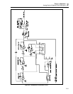
The mid stage is a common-emitter, Miller-compensated gain stage (Q5) that drives a
common-base level shifter (Q13) on the Oscillator Output assembly. This stage is
current limit protected by R12 and Q4. The dominant pole is set with the Miller
capacitor C5 and the input stage transconductance. The mid stage is biased to 10 mA by
Q6 and related components.
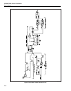
The output stage of the amplifier is a bootstrapped complementary Darlington pair. The
only parts of the output stage on this A13A1 assembly are the input transistors Q7 and
Q8. The output bias current is set by R17 and CR4-CR5 to be approximately 40 mA.
This keeps the output stage class A for all normal output conditions.
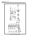
2-137. Output Stage
The output stage circuit is a complementary Darlington emitter follower bootstrapped
buffer amplifier. The input transistors are Q7 and Q8 on the A13A1 assembly. These
transistors drive the output transistors Q8 and Q14 respectively. Transistors Q10 and
Q11 in the positive side and Q16 and Q17 in the negative side are parallel transistors
bootstrapped by VR3 and VR4. Current sources CR13, CR14, CR17, CR18, CR15,
CR16, CR11, and CR20 provide the bias current for their respective bootstrapped
transistors. Current limiting for the positive side is provided by Q9 and R91. During an
overcurrent condition, the voltage drop across R91 turns on Q9, which draws current
away from the base of Q11. Current limiting is done in the same manner for the negative
side with Q15 and R99.
Switch S1 can be switched to pull the input of the A13A1 output stage low for
troubleshooting the output stage. Refer to the Oscillator Output troubleshooting section
for more information.
2-138. Phase Shifter
The phase shifter circuit provides a fixed amplitude variable phase auxiliary signal at the
rear panel of the calibrator. This signal is the same frequency as the output, but can be
phase shifted over a 360º range. The four phases (each 90º apart) for the oscillator circuit
are divided by Z4 and Z5. These signals are connected to the dual four-channel
multiplexer (U27), which is under the control of the PHASE control bus from the digital
control circuit. This multiplexer selects any two adjacent oscillator phases (e.g. 0º and
90º) that are connected to the input of a dual monolithic DAC U28. These signals are
then scaled by the dac (U28), also under the control of the digital control circuit. The two
outputs of this dac are summed by op amp U29. Using this method, the output of U29 is
a phase shifted signal between 0 and 360º, where the scaling of the signals phase shift
within a 90º range.
2-139. Power Amplifier Assembly (A16)
The Power Amplifier assembly outputs dc voltages from ±22V to ± 219.99999V and ac
voltages from 22V to 219.99999V rms. The frequency limit for 220V ac output is 100
kHz. Output voltage limits are derated at frequencies above 100 kHz. At 1 MHz, the
maximum output voltage is 22V rms. The Power Amplifier drives the High Voltage
assemblies (A14, A15) in all high voltage and high current functions.
This assembly also contains calibration circuitry that enables the internal calibration
system to determine exact Power Amplifier ac and dc gain, offsets and frequency
response.
The main sections of this assembly are the input stage, mid stage, output stage, sense-
current cancellation circuit, the dc and ac gain calibration circuits, and the Power
Amplifier Digital Control SIP assembly (A16A1), which is mounted on the Power
Amplifier assembly.