


5700A/5720A Series II Calibrator
Service Manual
2-86
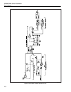
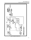
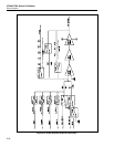
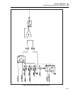
2-140. Power Amplifier Digital Control Sip Assembly (A16A1)
Digital control for the Power Amplifier assembly is contained on the SIP assembly
(A16A1) mounted at the bottom of the Power Amplifier. This assembly configures the
Power Amplifier assembly for its various modes of operation. (Also see "±PA Supplies
Digital Control" in the Power Amplifier Supply theory of operation.)
The heart of the Digital Control assembly is an 82C55 Programmable Peripheral
Interface IC (U11) operating under software control via the guarded digital bus. This IC
has three ports that generate 24 outputs. These outputs control two 5801 relay driver ICs
(U10, U12), two LM339 Comparators (U13, U15) and an analog multiplexer (U14) used
for diagnostics.
Relay driver U10 generates eight control lines (LC0*-LC7*) that control four latching
relays (K1-K4). Relay driver U12 generates eight control lines (C0*-C7*) for non-
latching relays K10-K17. C0* also controls FETs Q57 and Q58. Port A (PA0-PA7) from
U11 provides an input bus common to relay drivers U10 and U12. Each driver has
separate strobe and enable lines from port C of U11. Driver U10 is strobed by PC7 and
enabled by PC5. Driver U12 is strobed by PC4 and enabled by PC6. When a STROBE
line is selected, data on the bus (PA0-PA7) is strobed into the respective driver chip.
When an ENABLE is selected, this strobed data appears at the output, thereby energizing
the appropriate relays. Latching relays only need to be energized for 10 ms; non-latching
relays need to be energized continuously.
As an example, the following steps are taken to set up latching relays controlled by relay
driver U10.
1. Write the proper data for these relays to port A of the 82C55 (U11).
2. Write hex A to PC4-PC7 to strobe the data into U10.
3. Write hex 0 to PC4-PC7, wait 10 ms and write hex 2 to PC4-PC7. This takes U10's
output out of tri-state and energizes the proper relay coils for 10 ms. Since PC4 and
PC6 are always low, U12 is undisturbed.
Two LM339 quad comparators (U13 and U15) get their data from port B of U11 (PB0-
PB7) and generate control lines SW0-SW7. SW0-SW2 are inputs to decoder U9, which
generates eight additional control lines (CONT0*-CONT7*) for controlling FETs and
solid state switches. Control line SW3 controls FETs Q50 and Q51. Control lines SW4-
SW7 are routed through the motherboard to the Filter/Power Amplifier Supply assembly
(A18) to control the +PA and -PA supplies.
The diagnostic circuit enables the Calibrator to monitor eight diagnostic (MUX) signals
on the Power Amplifier assembly. A 4051 analog multiplexer (U14) is controlled by
PC0-PC3 from U11. This multiplexer selects of the eight MUX signals to the SDL line,
where it is measured by the adc circuit on the DAC assembly (A11). Resistor network Z2
and various resistors and zener diodes on the Power Amplifier assembly divide these
MUX signals down to a proper level for measurement by the adc circuit. The eight
monitored points are:
• MUX0 Output of U7; indicates the status of the amplifier loop
• MUX1 +PA Supply
• MUX2 -PA Supply
• MUX3 Power Amplifier output
• MUX4 Indicates the temperature of the Power Amplifier assembly
• MUX5 Power Amplifier dc input
• MUX7 Diagnoses the state of the hybrid heater-control circuit