


Theory of Operation
Analog Section Detailed Circuit Description
2
2-87
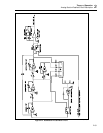
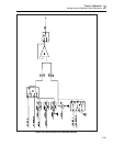
2-141. PA Common Circuitry
Common circuitry consists of the +PA and -PA supplies, input stage, mid stage, and the
output stage. These four circuits are described under the next four headings.
Power Amplifier input node, gain, and feedback are different for dc and ac operation.
Power Amplifier gain is -20 in the dc function, determined by the ratio of resistor
network bonded to the HR8 assembly (500 kΩ/25 kΩ). Gain in the ac function is -10,
which is determined by the ratio resistors [(R11 + R12 + R13)/R17]. This is described in
more detail under "DC Voltage Function" and "AC Voltage Function".
2-142. +PA and -PA Supplies
The ±PA supplies are high voltage supplies generated by the Filter/PA Supply assembly
(A18). These supplies can be controlled by the Digital Control SIP assembly (A16A1)
and are switched between the two modes shown in Table 2-13.
• ±185V
• ±365V
Theory of operation for the Filter/PA Supply assembly (A18) describes how these
voltages are generated and selected.
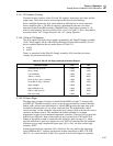
Table 2-13. PA and -PA Supply Settings at Different Outputs
Calibrator Output +PA -PA
Less than 22V ac or dc +185V -185V
22 to 110V dc +185V -185V
110 to 220V dc +365V -185V
-220 to -110V dc +185V -365V
22 to 101V ac (freq < 120 kHz) +185V -185V
22 to 85V ac (freq > 120 kHz) +185V -185V
Other voltages +365V -365V
220 to 550V dc or ac +185V -185V
550 to 1100V dc or ac +365V -365V
220 mA to 2.2A +365V -365V
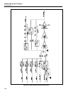
2-143. PA Input Stage
The input stage consists of a heater-controlled hybrid HR8, op amp U7, transistor Q6,
and JFET Q2. The HR8 assembly consists of an op amp mounted on a heated-substrate
hybrid, with a resistor network bonded to it. Hybrid HR8 provides the input stage with
excellent dc characteristics of low offset, noise and drift. The hybrid heater-control
circuit (on sheet 3 of the schematic) adjusts the base voltage of Q38 to deliver the correct
current to the heater resistor. This maintains the hybrid assembly at a constant
temperature in spite of environmental temperature variations. Transistor Q35 protects the
hybrid in case Q38 fails. Input of the hybrid op amp is protected by CR13 and CR14.
Output of the hybrid op amp is connected to the input of a faster op amp (U7), which
provides additional dc gain and a higher slew rate. JFET Q2 and transistor Q6 combined
with these two op amps complete the input stage. Q2 is a very low-bias-current, high-
frequency JFET.
In mid to high-frequency operation, Q2 is effectively the only path for the input stage
signal. HR8 and the U7 op amps are bypassed at these frequencies by R89, C42, R24,
and C12. As a result, the base of Q6 is at ac ground. In dc to mid-frequency operation,