


5700A/5720A Series II Calibrator
Service Manual
2-122
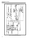
Relay driver U11 controls the three non-latching relays K14, K15, and K17 on this
assembly. It also generates control line RLY11* to control K11 on the Motherboard.
Relay K11 routes I-GUARD, described later, to the rear panel for operation when the
rear-panel binding posts are in use.
The diagnostic circuit allows the calibrator to monitor five points on the assembly.
Points DUMMY LOAD, OVEN TEMP, and CUR/COMP MONITOR are from the
Current section. Points HI-RES LOOP and HI-RES CLOCK come from the Hi-Res
section. Outputs PB0-PB2 select which point the multiplexer U12 monitors. PC6 enables
the output of U12 to the SDL line, where it is measured by the adc circuit on the DAC
assembly (A11).
Outputs PB3-PB5 generate control lines FET3, FET1, and FET2 respectively, which are
used by the Current section. FET1 controls NMOSFETs Q21 and Q22, FET2 controls
Q20 and Q23, and FET3 controls quad CMOS analog switches U5A, U5C, and U5D.
Output PB7 generates control line FET4, which controls analog switch U5B.
Outputs PB6 and PC7 generate control lines HI-RES RANGE and HI-RES ON/OFF
respectively, which are used by the Hi-Res section. These lines control quad CMOS
analog switch U18 and comparator U13.
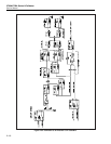
2-187. Current Section
The current section of the A7 assembly uses dc voltage from the DAC assembly and ac
voltage from the Oscillator Output assembly to generate both ac and dc current outputs.
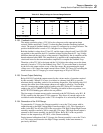
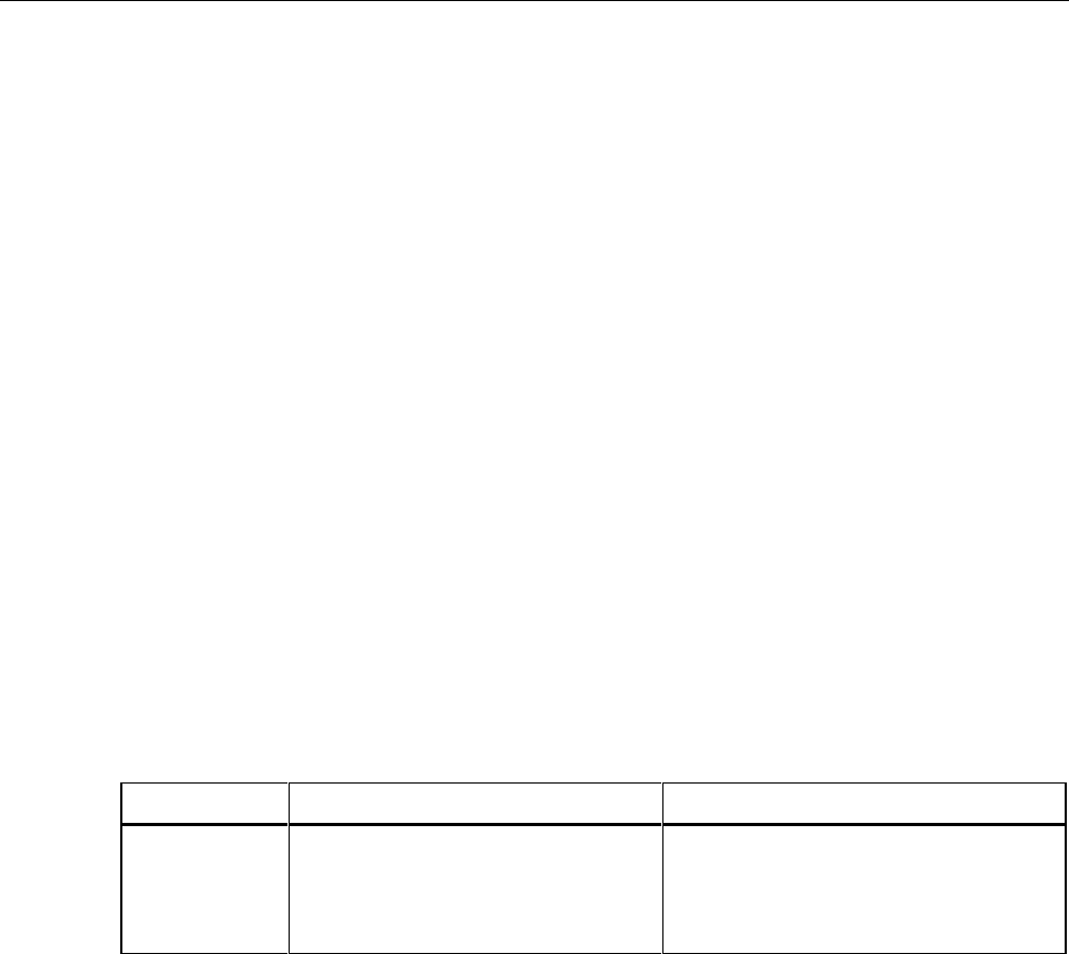
Four ranges of output current each for ac and dc are generated as shown in Table 2-14.
AC current is available from 40 Hz to 10 kHz.
Table 2-14. AC and DC Current Ranges
Range DC Current Limits AC Current Limits
220 µA 0 to 219.9999 µA 9.000 µA to 219.999 µA
2.2 mA 0.220000 mA to 2.199999 mA 0.22000 mA to 2.19999 mA
22 mA 2.20000 mA to 21.99999 mA 2.2000 mA to 21.9999 mA
220 mA 22.0000 mA to 219.9999 mA 22.000 mA to 219.999 mA
The 2.2A range is generated on the High Voltage/High Current assembly (A15) and
routed to this assembly for switching to the OUTPUT binding posts. This is further
described under the heading, "2.2A Range."
The transconductance amplifier, shunt resistors, feedback loop, and complementary
drive circuits form a loop to create the output current. In addition to these circuits, the
Current assembly contains input switching, output switching, a current guard, and a
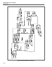
current/compliance voltage monitor. Each of these circuits is described in detail. To
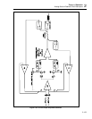
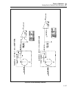
better understand the theory of operation, refer to Figure 2-35 and the schematic.
2-188. Current Input Switching
Relay K1, CMOS analog switch U5B, and FETs Q20-Q23 select the input source
voltage. For dc operation, the 22V range of the DAC assembly (A11) is brought in on the
B IN and B FB lines from the Switch Matrix assembly (A8). For ac operation, the 22V
range of the Oscillator Output assembly (A13) is brought in on the B IN and B FB lines.
During calibration of the current functions, the 13V buffered dc reference BRF13 and
BSRF13 are selected when K1 is set and U5B is closed.