


Theory of Operation
Analog Section Detailed Circuit Description
2
2-121
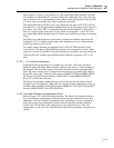
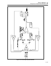
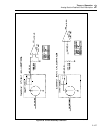
2-185. Calibrating to the External 1W Standard
The 1Ω and 1.9Ω resistor values are calibrated by comparing them against a 1Ω external
standard. The technique used is different from that used for the 10 kΩ external standard.
The Current assembly supplies a 130 mA (65 mA for 1.9Ω calibration) current through
both resistors. This current goes out the OUTPUT HI binding post to the 1Ω standard. It
comes back in through the OUTPUT LO binding post and through the internal 1Ω
resistance by K26 and K6, or 1.9Ω by K26 and K30 before going to S COM through
K22.
For the first reading, the inputs to the differential amplifier are connected across the
sense points of the 1Ω standard. Relay K1 connects the differential amplifier +input to
OHMS SENSE HI, which is connected to INT SENSE HI by K16 and K2 on the Ohms
Main assembly. INT SENSE HI is connected to the SENSE HI binding post by relays on
the motherboard. Relay K13 connects the differential amplifier -input to INT SENSE LO
which is connected to SENSE LO binding post by relays on the Switch Matrix assembly.
The voltage between the inputs is 0.13V, which is amplified by 75 by the differential
amplifier to approximately 9.75V and sent to the DAC assembly on the RCL line.
Another differential amplifier on the DAC assembly compares the 9.75V to the DAC
output. Before the reading is taken, however, amplifier offsets are determined.
When the DAC output equals the output of the differential amplifier on the Ohms Cal
assembly, the reading is stored and a second reading is taken. For this reading, the inputs
to the differential amplifier on the Ohms Cal assembly are connected across the 1Ω or
1.9Ω on the Ohms Cal assembly. The +input of the differential amplifier is connect
through K1 and K4 and the -input is connected through K2 and FET Q4. The second
reading is taken the same way as the first. The ratio of the two DAC settings are equal to
the ratio of the values of the two resistors. The value of the 1Ω and 1.9 ohm resistors are
determined from this ratio and the value of the external standard.
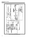
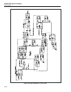
2-186. Current/High Resolution Oscillator Assembly Overview (A7)
The Current/Hi-Res (High-Resolution Oscillator) Assembly combines two functions on
one circuit board. The Current section generates dc and ac currents in the range of 20 µA
to 220 mA. The Hi-Res section generates a high-resolution signal accurate in frequency
to 4 1/2 digits, which is used by the phase-locked loop circuit on the Oscillator Output
assembly (A13). These two functions are independent circuits except for the sharing of
some digital controlling and self-diagnostic monitoring. The following theory describes
the digital control circuitry used by both circuits, then independently covers the Current
and Hi-Res functions.
The heart of the Current/Hi-Res assembly digital control circuitry is a 82C55
Programmable Peripheral Interface IC (U7), which is under software control via the
guarded digital bus. This IC has three ports which generate 24 outputs. These outputs
control three UCN5801 latching relay drivers ICs (U8-U10), a UCN5800 relay driver
(U11) for controlling non-latching relays, a 4051 analog multiplexer (U12) for self
diagnostics, and several FET switches throughout the assembly. Port A (PA0-PA7) is a
common input bus called CONTROL BUS on the schematic. This CONTROL BUS
transmits the desired state of all the relays (K1-K17) in the Current section, and also to
control two synthesizer ICs (U16, U17) in the Hi-Res section.
Four relay driver ICs drive latching controlling relays K1-K13 and K16. The CONTROL
BUS (port A of U7) is a common input bus. Port C of U7 (PC0-PC5) provides the strobe
and enable lines for these relay drivers. PC0 enables U8, while PC1 enables U9 and U10.
PC2, PC3, PC4, and PC5 strobe U11, U8, U9, and U10 respectively.