


Theory of Operation
Analog Section Detailed Circuit Description
2
2-133
5220EN* is the output enable for octal latch U10. 5220ADIR* is the output enable for
buffer U11. 5205EN* is the output enable for octal latch U9.
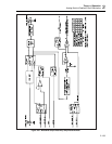
2-210. Auxiliary Amplifier Interface
A 5725A amplifier can be physically connected to the 5700A/5720A Series II. Only one
can be used at a time. Depending on the amplifier’s mode of operation, the output of the
Calibrator is either an ac or a dc voltage.
2-211. 5725A Interface
The Calibrator is designed to work in close connection with the 5725A Amplifier. The
rear panel in this system provides relay switching for the 5725A signals. All voltage
outputs from the 5725A are routed back to the binding posts on the Calibrator. All
current outputs from the 5725A are sourced at the 5725A OUTPUT binding posts. You
can configure the Calibrator to also source all its current outputs through the 5725A
OUTPUT binding posts for convenience.
Connector J8 and Cable 4406 interface all the Calibrator I/O signals between the
Motherboard and the rear panel. Connector J7 interfaces the Calibrator to the 5725A
Amplifier. The interface between these two connectors is accomplished through relays
K1, K2, and K6-K9. Relays K6-K9 break all the I/O lines except B-SENSE HI, B-OUT
HI, V-GUARD, and B-IGRD, and connect them all to V-GUARD when the 5725A is not
in use.
During 5725A operation, relays K1, K2, K6, and K7 switch the Calibrator analog signals
B IN, B FB, B SNSLO, and PACOM to lines BOOST IN, B-FEEDBACK, B-SENSE
LO, and BPA COM on connector J7.
High voltage output of the 5725A (B-OUT HI and B-SENSE HI) is connected to the
Calibrator Motherboard via cable 4406 where it can be switched to the Calibrator
binding posts by relays on the motherboard.
Relays K8 and K9 connect the 5725A current function lines I-RET, and B-CUR on
connector J8 to B-IRTN, and B-CURRENT, on connector J7 when the 5725A is
outputting Calibrator current (≤2.2A). Line B-RCL is used during 5725A calibration.
Line B-RCL on J7 is connected to J8 through relay K6. Line B-RCL is routed via the
motherboard to the Current assembly (A7) where it is switched to the calibrator RCL
line by a relay.
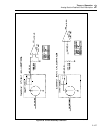
2-212. Phase Lock In/Variable Phase out
The Oscillator Output assembly (A13) can be phase locked to an external signal
connected to the PHASE LOCK IN BNC connector J6. Relay K10B connects the shell of
this BNC connector to chassis ground through protection resistor R19 when the
Calibrator is on internal operation, or to P LOCK LO when the Calibrator is phase
locked to the external signal coming in on J6.
This incoming signal is called PHLK IN on the schematic. Relay K10A switches an
external phase-lock signal from J6 to the input of Q1 and Q2. FETs Q1 and Q2 provide
current limiting for PHLK IN. Signal P LOCK is routed to connector J8 where it is
connected to the Oscillator Output assembly via the Motherboard.
Components CR1, CR2, VR1, VR2, R4, and R5 provide amplitude protection for the
phase lock circuitry on the Oscillator Output assembly by limiting the amplitude of P
LOCK.
The Variable Phase Out BNC connector (J5) is connected to P SHIFT and its shell is
connected to PA COM by energizing relay K12. Signal P SHIFT is a fixed-amplitude
variable phase signal generated by the Oscillator Output assembly (A13). Refer to the