


5700A/5720A Series II Calibrator
Service Manual
2-134
Oscillator Output assembly theory of operation for a detailed description on the
generation of P SHIFT. Resistor R18 serves as overcurrent protection for the BNC shell
connection on J5.
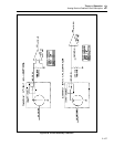
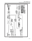
2-213. Rear Panel Relay Control
The relays on the Rear Panel assembly are used as the interfaces for the 5725A
amplifier, or for switching the PHASE LOCK IN and VARIABLE PHASE OUT signals.
The relay switching circuitry is under control of the guarded digital bus via connector J8.
This guarded digital bus is generated on the Regulator/Guard Crossing assembly (A17).
The relay control circuitry is located on sheet 5 of the Rear Panel schematic. This circuit
uses an 82C55 programmable peripheral interface (U14) and two relay drivers (U16 and
U17) to control the 12 relays on this assembly and one relay (K12) on the Analog
Motherboard. The 82C55 (U14), which is under control of the guarded digital bus via
connected J8, has three ports generating 24 outputs.
Port A (PA0-PA7) provides the input lines for relay driver U16.
Port B (PB0-PB7) provides the input lines for relay driver U17.
PC0-PC2 of port C provides the CLEAR, STROBE, and OUTPUTENABLE lines for
these relay drivers.
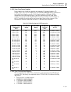
Relay Driver U16 controls two latching relays (K2 and K3) and four non- latching relays
(K1, K4, K5, and K7). Relay driver U17 controls one latching relay (K6) and five non
latching relays (K8-K12). Relay driver U17 also creates control line RLY12* (pin 13)
which controls relay K12 on the Analog Motherboard assembly (A3).
2-214. Rear Panel CPU Interface
The rear panel is interfaced to the CPU assembly (A20) via connector J8 on the rear
panel. The CPU has:
• Five address lines (RPA1-RPA5) which comprise the ADDRESS BUS