


Theory of Operation
Digital Section Detailed Circuit Description
2
2-27
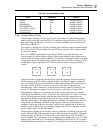
2-42. Clock Filter Circuit
The clock filter circuit generates a 3.6864 MHz 200 mV sine wave for the Rear Panel
and Front Panel assemblies. This circuit buffers the 3.6864 MHz Clock with an inverter
in U3. The circuit contains dc-blocking capacitor C80, two stages of a low pass LC filter
(L80 and C81, L81 and C82), transformer T51, and termination resistor R82.
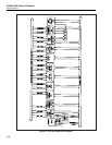
2-43. CPU to Rear Panel Interface
Components U25, U26, U27, and connector P62 interface the CPU to the rear panel. Bi-
directional bus transceiver U26 buffers the data lines. Signal R/WR* controls the
transmission direction of the data lines, and RRPNLEN* is the chip enable. IC U25
buffers control lines BRPDRTINT*, BRPIEEEINT*, and BRPDTK*. U27, enabled by
RRPNLEN*, buffers address line A01-A05 and control lines WRL* and R/WR*.
Control lines RESETL, RPSEL*, TXDB, RCVB, and XMT go directly to connector P62.
2-44. CPU to Front Panel Interface
Components U25, U28, U29, U30 and connector P61 interface the front panel to the
CPU. Bi-directional bus transceiver U30 buffers the data lines. Control signal R/WR*
controls the transmission direction of the data lines, and FRNTPNLEN* is the chip
enable. IC U28, enabled by FRNTPNLEN*, buffers address lines A05-A12. IC U29, also
enabled by FRNTPNLEN*, buffers address lines A01-A04 and control line R/WR*. Two
sections of U25 in parallel buffer IORESET*, providing twice the drive current of a
single section, generating BRESET*. Three other sections of U25 buffer FPINT*,
FPDTK*, and PSFAILINT*. Control line FRNTPNLCS* goes directly to connector P61.
2-45. Fan Monitor
The fan monitor circuit detects whether one of the two fans is fully or partially shorted,
open-circuited, or drawing excessive current. Current-sense resistors on the Digital
Motherboard send analog signals FAN1 and FAN2 to the CPU through P61. FAN1 is
subtracted from FAN2 in U52D, and the difference is amplified before being sent to a
window comparator made up of U52B and U52C (plus associated resistors). Capacitors
C12 and C13 act as low-pass filters for the two signals, preventing spurious noise from
interfering with detection circuitry.
When the output of U52D is greater than +5V, the output of U52B goes low (to about -
11V); otherwise the output is high (about +11V). U52A takes the +5V and generates a -
5V reference for comparator U52C. When the output of U52D is more negative than -
5V, the output of U52C goes low (to about -11V); otherwise the output is high (about
+11V). The outputs of U52B and U52C are wire-ORed through CR2 and CR3, using
R52 and R53 to limit current sunk by the comparators when their respective outputs are
low. Schottky barrier diode CR4 converts the -11V outputs of the comparators, when
either is low, to a TTL-level logic low, which is the active (true) level of FANINT*.
When both fans are functioning properly, diodes CR2 and CR3 are reverse-biased,
effectively taking the comparators out of the circuit. At this point, R51 pulls FANINT*
to a valid TTL-level logic high, the inactive state of FANINT*. R51 and CR4 level-shift
the ±11V signal to valid TTL levels.
Signal FANINT* goes to DUART U31 and to the interrupt controller U10 for further
processing. System software monitors FANINT* through U31, and can program the
DUART to generate a GCDUARTINT* interrupt signal on FANINT* going low.