


Theory of Operation
Digital Section Detailed Circuit Description
2
2-21
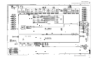
2-30. CPU (Central Processing Unit) Assembly (A20)
The CPU (Central Processing Unit) for the Calibrator is a single-board computer based
on a 68HC000 microprocessor. The CPU assembly communicates with the Guarded
Digital section, the Front Panel assembly, and the Rear Panel assembly. The board can
be divided into three primary areas:
• The microprocessor and its support circuitry
• Memory
• Peripheral chips and I/O interfaces
Microprocessor support circuitry consists of a power-up and reset circuit, clock
generation, a watchdog timer, address decoders and DTACK (data acknowledge)
generator, bus error timeout, and interrupt controller.
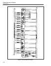
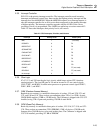
Figure 2-5 is a block diagram of the CPU assembly. Table 2-3 is a glossary of the
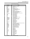
acronyms used in the text and schematic for the CPU assembly.
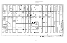
2-31. Power-Up and Reset Circuit
The power-up and reset circuitry consists of line monitor chip U1, C5, C6, CR1, R3, Z3,
switch SW1, and inverters on U2. This circuit provides a 195 ms reset pulse at power-up
or upon pressing and releasing SW1, placing the CPU assembly in a known safe
condition. If the power supply glitches or falls below 4.55V ±0.05V, U1 resets the
Calibrator. The reset pulse duration is determined by C5. Note that SW1 performs a
different function than the front panel RESET button. SW1 is a hardware reset that is
hard-wired to and directly read by the microprocessor. The front panel RESET button is
a software reset; it tells the system software to restore the Calibrator configuration to a
default condition.
The heart of this circuit is the line monitor chip U1. On power-up or when SW1 is
pushed, U1 forces an active-low reset pulse on RESETL and an active-high pulse on
RESET. RESETL helps to prevent accidental writes to EEPROM and drives an inverter
in U2 to turn off LED CR1. CR1 indicates that the +5V supply is on and that the CPU is
operating, i.e. not reset. RESETL also resets the rear panel assembly. The other output,
RESET, drives two inverters in U2. One of these inverters provides HALT*. The other
generates IORESET*, which drives the processor's RESET, and provides a reset for the
front panel interface and DUARTs (dual universal asynchronous receiver/transmitter)
circuitry.
2-32. Clock Generation
The clock generation circuit uses components Y1, Y2, U3, U4, R4, R5, C8, C9, and E5.
The crystal Y1, along with the resistors, capacitors, and an inverter in U3 generates the
7.3728 MHz primary system clock CLK. This system clock is used by the processor and
is divided down by a binary counter (U4) for clocks of 3.6864 MHz, 28.8 kHz, and 450
Hz. The 450 Hz clock is used by the watchdog timer, the 28.8 kHz is used by U6 in the
decoding circuit, and the 3.6864 MHz is used by the DUARTs, and the clock filter
circuit. Jumper E5 allows for selection of the alternate oscillator (Y2) as the system
clock.