


5700A/5720A Series II Calibrator
Service Manual
2-140
2. The second range is for operation at frequencies between 12 kHz and 1.1 MHz. In
this mode the input signal is also from the Oscillator Output assembly, but the
amplitude is controlled by the amplitude control circuit on the Wideband Output
assembly. Relay K10 is in the set position to connect the output of the rms sensor
and amplitude control circuit to the RCL line where it is measured by the adc circuit
on the DAC assembly. The DAC assembly operates in conjunction with the
Oscillator Control assembly to adjust the amplitude of the Oscillator Output signal.
3. The third range is for operation at frequencies between 1.2 MHz and 30 MHz. In this
mode the input signal is from the Wideband Oscillator assembly via connector J1. Its
amplitude is controlled by the amplitude control circuit on the Wideband Output
assembly. In this mode, the output of the DAC assembly, DAC OUT HI and DAC
SENSEHI, are connected to DAC OUT by relay K11 in the set position. Op amp
U12B compares DAC OUT to the output of the rms sensor and amplitude control
circuit. Any difference between these two signals is amplified and routed to the
Wideband Oscillator assembly via the AMPLITUDE CONTROL line. The
Wideband Oscillator uses the Amplitude Control line to adjust its AC amplitude
until the sensor output is equal to the DAC voltage.
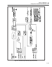
2-223. Wideband Output Power Amplifier Circuit
The power amplifier circuit, as outlined on sheet 1 of the Wideband Output assembly
schematic, contains all the circuitry shown on sheet 2 of the schematic. This circuitry
consists of the x10 amplifier, the unity-gain amplifier, and the 10 Hz to 1.1 MHz buffer
circuit as outlined on the schematic.
The x10 amplifier circuit is used only during operation in the 1.2 MHz to 30 MHz range.
The 1.2 MHz to 30 MHz sine wave input comes from the Wideband Oscillator assembly
via a coaxial cable and connector J1. This input signal has a nominal full-scale amplitude
of 700 mV rms.
The x10 amplifier circuit uses transistors Q4, Q5, Q6, Q7, Q8, Q9, and Q10 to amplify
this signal by a factor of 10. Amplifier U11A keeps the DC offset on the output to near
zero. The output of the X10 amplifier is applied to the unity gain amplifier by relay K12
in the reset position. The output impedance of the unity gain amplifier is 50Ω, therefore
the x10 amplifier must produce 7.0V rms to give 3.5V rms into the 50Ω load.
The 10 Hz to 1.1 MHz buffer circuit is used during operation in the 10 Hz to 12 kHz
range or the 13 kHz to 1.1 MHz range. In this mode, the input signal comes from the
Oscillator Output assembly. This input signal is buffered by Q17 and applied to relay
K12. Amplifier U11B keeps the DC offset on the output near zero for the 10 Hz to 1.1
MHz range.
The unity-gain amplifier is connected to either the output of the x10 amplifier or the
output of the 10 Hz to 1.1 MHz Buffer by relay K12. The unity gain amplifier uses
transistors Q11-Q16 and associated components. This circuit increases the power to a
level that drives 3.5V rms into a 50 ohm load. The four 1/2-watt resistors in parallel
(R96, R97, R98, R99) along with the output resistance of the amplifier form the 50Ω
output resistance.
The output of this amplifier, called 10HZ TO 30MHZ OUTPUT, is a sine wave with an
amplitude between 1.1V and 3.5V rms into 50Ω. This output signal is used by the
attenuators to provide the overall output range of the Wideband Output assembly.
Resistors R41 and R42, and capacitor C23 divide this output signal to create OUTPUT
OFFSET for diagnostics.