


Theory of Operation
Analog Section Detailed Circuit Description
2
2-65
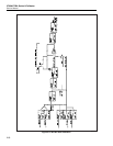
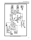
The reference circuit is designed such that the effects of the thin-film resistors and op
amp errors are second order. Thus, accuracy is determined almost entirely by the ref
amps.
To further reduce the effects of ambient temperature variations, the hybrid is heated to a
constant 62ºC by the heater control circuitry on sheet 1 of the DAC schematic.
Temperature is sensed near the ref amps by a thermistor (RT1). If the substrate
temperature changes, the thermistor resistance changes. This creates a correction voltage
to the base of Q2 (on the main board). This, in turn, causes the power into the heater
resistor, which is screened on the back of the substrate, to increase or decrease as
necessary to maintain a stable temperature.
Thermal runaway is prevented by a protection circuit. Once the substrate temperature
reaches approximately 67ºC, the change in resistance of RT2 causes Q9 to turn on. As
transistor Q9 turns on, it steals base current from Q1 on the main board, which brings it
out of saturation. This breaks the current path through the heater resistor. This condition
exists only if there is a failure.
The exact value of the reference is determined during calibration. Because of the
stability of the reference, it can be used for future internal calibration procedures to
remove short term errors in the calibrator.
The 13V output, REF13 HI, is from pin 9 and REF13 SENSE is on pin 12. Also, a 6.5V
reference line, REF6, is brought out on pin 14 of the reference for use during calibration.
In order to make these reference voltages available to other assemblies, the 6.5V and
13V references are buffered on the DAC Buffered Reference SIP assembly (A11A2).
This assembly also contains the circuitry to switch the references and buffered references
into the input of the adc during calibrator calibration. Refer to the section on the DAC
Buffered Reference SIP for more information.
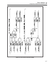
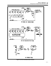
2-104. Duty-Cycle Control Circuit
Duty-cycle control circuitry is pictured on sheet 3 of the schematics. DAC output
voltages are represented in software by what are called first and second channel counts.
Each count is a 16-bit number which is sent to the DAC assembly via the guarded digital
bus.
For example, a first channel count of 20,000 (in decimal) represents a DAC output
voltage of approximately 6.5V (half the reference voltage).
The first function of the duty-cycle control circuitry is to convert each count into a
stable, TTL level, square wave, with a duty cycle proportional to the numeric value of
the count. This is accomplished with the 82C54 programmable interval timer (U6).
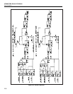
A low-level 8 MHz clock is generated on the Regulator/Guard Crossing assembly (A17)
and routed to the DAC assembly via the motherboard. This low-level clock, CLK and
CLK*, is amplified to a TTL level by comparator U7 to generate the 8 MHz clock which
is used by U6 and the adc IC U25.
The 82C54 programmable interval timer receives its input counts from the guarded
digital bus and creates the second channel signal on OUT2 (pin 20) and the first channel
signal on OUT1 (pin 16).
The second channel signal is buffered by U8 (D and E) and runs through opto-isolator
U12 to become CH2 FLOATING. This signal alternately turns FETs Q30 and Q32 on
and off to turn the 3V source (called 3V) into a floating 3V pulse width modulated
waveform called CH2 FILTER INPUT.