Troubleshooting
Component-level Troubleshooting
5
5-67
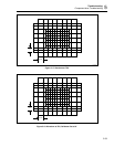
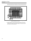
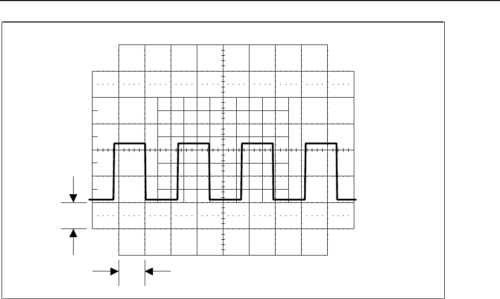
1 V
10 ms
F5-26.EPS
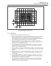
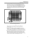
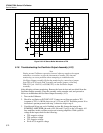
Figure 5-26. Waveform at Pin 7 of U12
5-15. ADC Circuit
Proceed as follows to troubleshoot the ADC circuit:
1. Check the ADC INPUT select circuit. Set the Calibrator to 10V dc, operate. Verify
that the voltage at U23 pin 7 (common to TP12) is 0.45V±7%. If this voltage is
incorrect, check U23 and its control lines. At this time DAC HI DIAG is divided by
R79 and R84 (0.45V)and selected by control line DAC DIAG SEL.
2. Check the ADC INPUT. Set the Calibrator to 10V dc, operate. Verify that the
voltage at U25 pin 22 (common to TP12) is 0.45V±7%. If this voltage is incorrect,
check U24 and its associated components.
3. Check the buffered DAC LO DIAG. Set the Calibrator to standby. Verify that the
voltage at U22 pin 6 (common to TP1) is 0V±11 mV. If this voltage is incorrect,
check U22 and associated components.
4. Check the ADC +7.5V supply. Set the Calibrator to standby. Verify that the voltage
at U25 pin 16 (common to TP1) is 7.5±0.5V. If this voltage is incorrect, check VR27
and R77.
5. Check the ADC -8.2V supply. Set the Calibrator to standby. Verify that the voltage
at U25 pin 17 (common to TP1) is -8.2±0.5V. If this voltage is incorrect, check
VR28 and R94.
6. Check the BUFFERED ADC COM. Set the Calibrator to standby. Verify that the
voltage at U26 pin 7 (common to TP12) is 0V±600 mV. If this voltage is incorrect,
check U20B, U26A, and associated components.
7. Check the ADC -6.4V Reference. Verify that the voltage at the anode of VR29
(common to TP12) is -6.4±0.2V. If this voltage is incorrect, check VR29, VR30,
U20B, U26A, and associated components.


